Method of manufacturing a surface acoustic wave device

a surface acoustic wave and manufacturing method technology, applied in the direction of electrical transducers, transducer types, piezoelectric/electrostrictive transducers, etc., can solve the problems of poor dimensional accuracy, curved upper surfaces, and difficulty in forming with a uniform height, so as to prevent mounting failure

Inactive Publication Date: 2005-02-01
PANASONIC CORP
View PDF30 Cites 5 Cited by
  • Summary
  • Abstract
  • Description
  • Claims
  • Application Information

AI Technical Summary

Benefits of technology

The present invention addresses the above issues and aims at providing a SAW device that can prevent mounting failure when mounting a SAW element in a package.
In order to attain this object, the SAW device of the present invention comprises a package having an external terminal, a SAW element housed in the package, and a lid for sealing opening of the package, wherein the SAW element further comprises on the surface of a piezoelectric substrate at least an IDT electrode, a connection electrode electrically connected to the IDT electrode, and an acoustic absorber formed on the outside of the IDT electrode, that is, on an end portion of the piezoelectric substrate, in a manner such that its top surface is parallel to the main surface of the piezoelectric substrate. As the surface of the acoustic absorber is parallel to the main surface of the piezoelectric substrate in this way, and as the top surface of the acoustic absorber is a plane, it is easy to suck the SAW element with a vacuum chuck when mounting in a package and it is possible to securely mount it at a predetermined position of the package.

Problems solved by technology

When the acoustic absorbers 103 are formed by screen printing in this manner, the dimensional accuracy is poor and also their cross sections become dome-like due to drips caused by flow of the resin, thus suffering from the upper surfaces becoming curved and difficulty in forming with a uniform height.
In addition, piezoelectric substrate 100 may incline relative to the bottom surface of the package 107 thus presenting a possibility of causing mounting failure.
In this case, too, there is a possibility of causing connection failure when the heights of the acoustic absorbers 103 are non-uniform and are greater than the bumps 111.

Method used


Image

  • Method of manufacturing a surface acoustic wave device
  • Method of manufacturing a surface acoustic wave device
  • Method of manufacturing a surface acoustic wave device

Examples


first exemplary embodiment

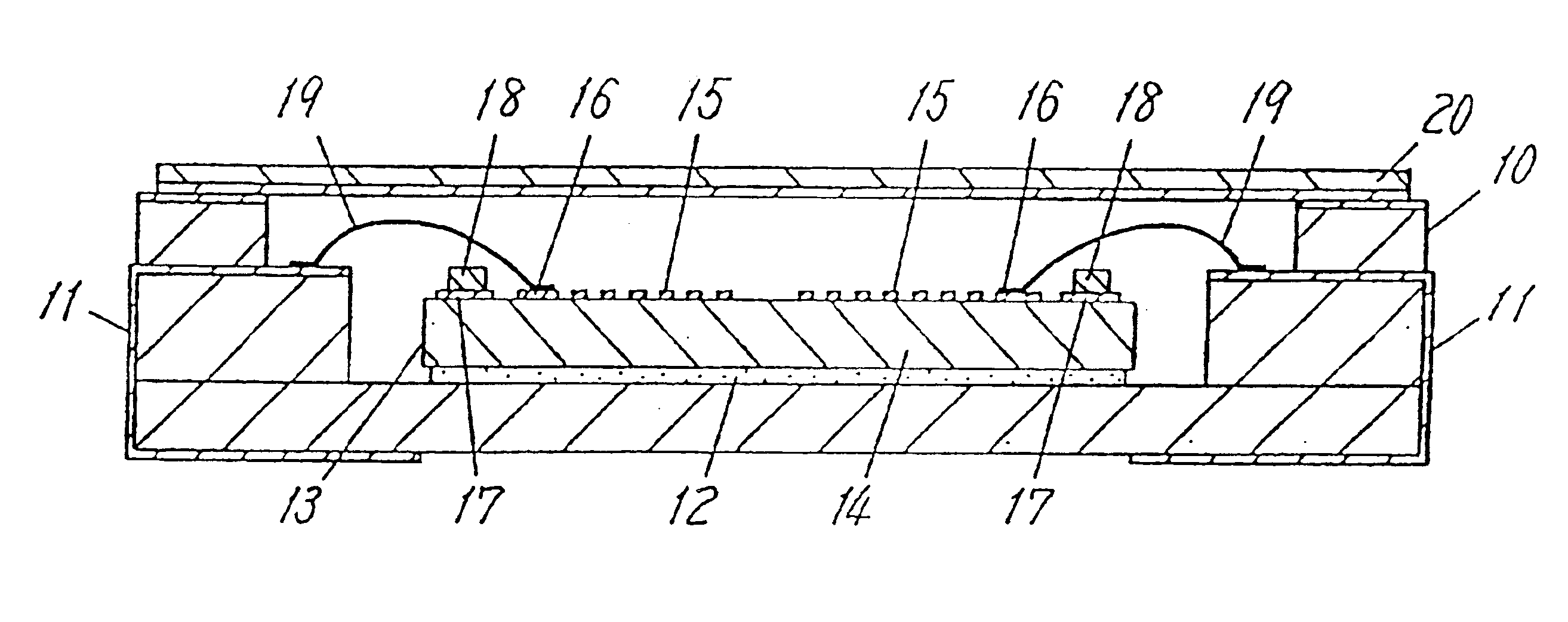
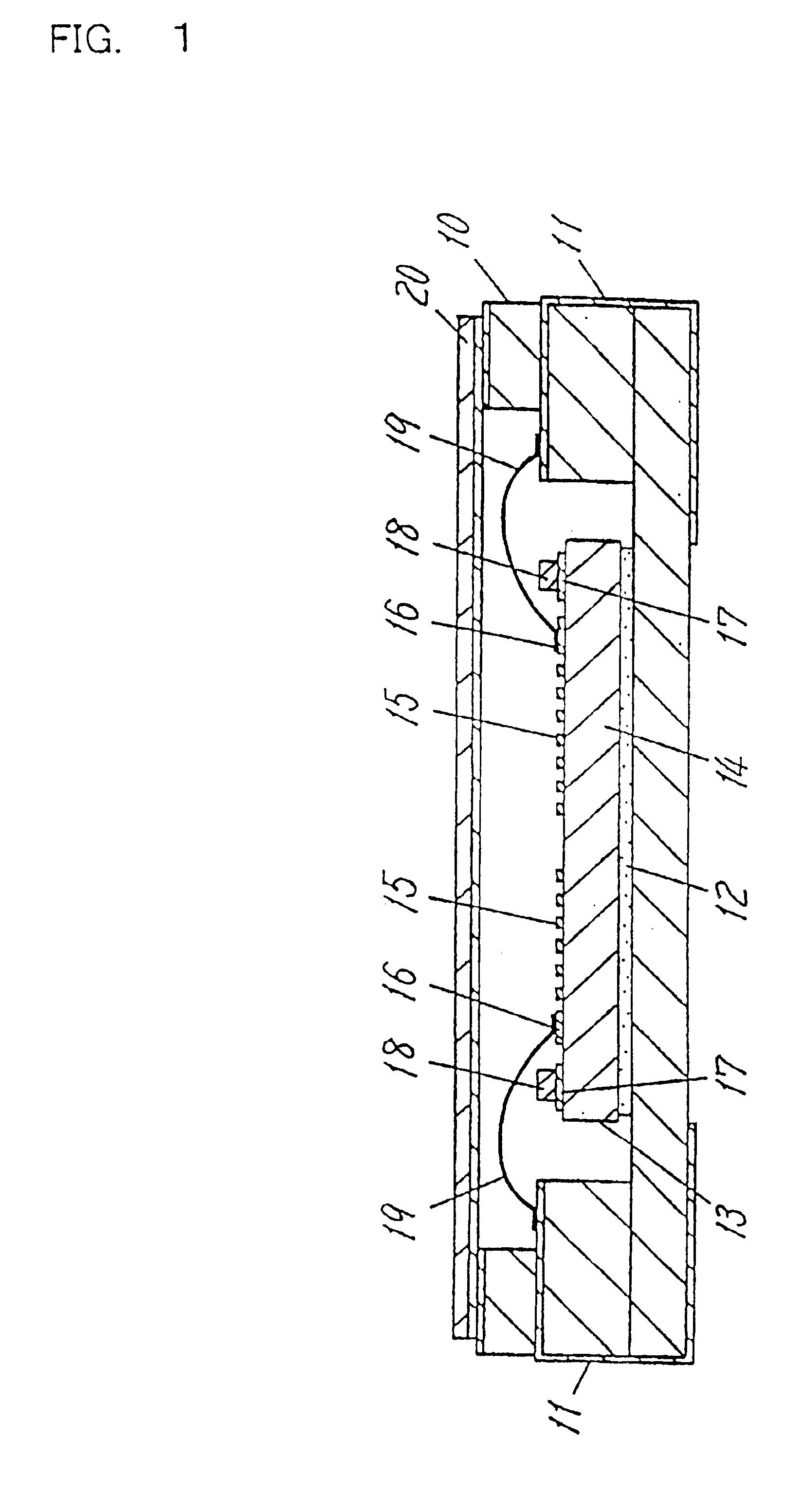
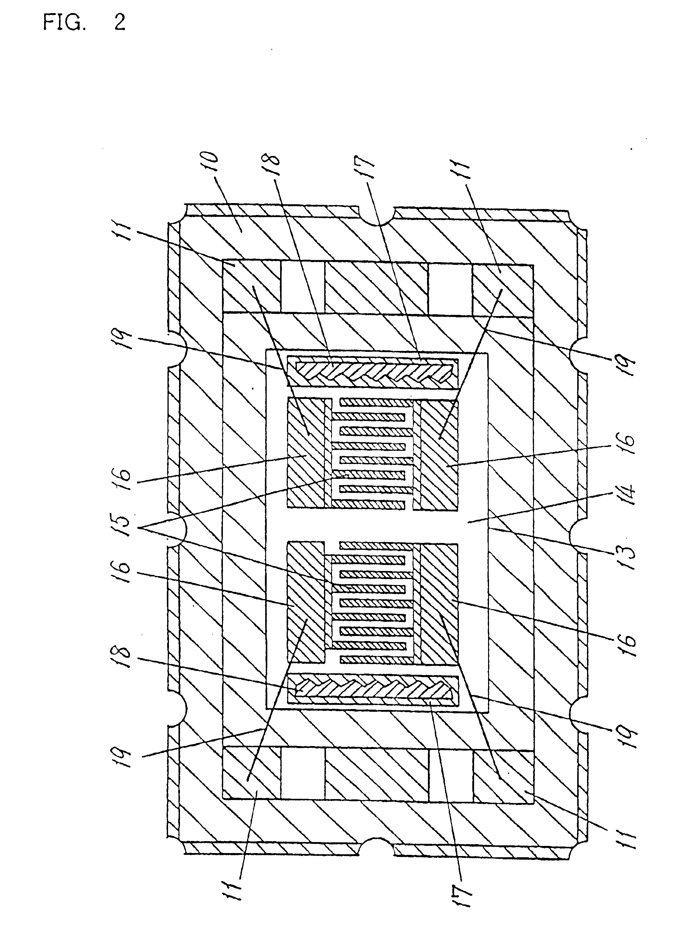
Referring to FIGS. 1 to 3, a description will be given on a first exemplary embodiment of the present invention.

A uniform thickness vapor deposited film composed of aluminum or a metal having aluminum as the main constituent is formed on the main surface of a wafer composed of a piezoelectric material such as quartz, LiTaO3, LiNbO3, and the like. Positive type photoresist is then uniformly coated by spin coating on top of the vapor deposited film. Next, the photoresist is exposed and developed so as to make IDT electrodes 15 having a desired shape, connection electrodes 16 to be connected to the IDT electrodes 15, and underlying metal layers 17 to be disposed at the locations where acoustic absorbers are to be formed, and then the vapor deposited film is etched to obtain IDT electrodes 15, connection electrodes 16, and underlying metal layers 17, and the photoresist is removed. Here, the underlying metal layers 17 are formed to a size greater than the acoustic absorbers to be formed...

second exemplary embodiment

Referring to FIGS. 4 and 5, a description will be given on a second exemplary embodiment of the present invention.

First, a plurality of SAW elements 13 having IDT electrodes 15, connection electrodes 16, and underlying metal layers 17 are formed on a wafer in a manner similar to the first exemplary embodiment. Next, a coupling layer 21 is formed by uniformly spin coating a silane-based underlying coupling agent over the entire surface on the side of the wafer where the IDT electrodes 15 have been formed. Subsequently, solvent component in the coupling layer 21 is removed by drying.

Afterwards, as in the first exemplary embodiment, the entire main surface of the wafer is covered with a negative photoresist film, which is then pressed while being heated. As the film resist, one having the same thickness as the thickness of the acoustic absorbers 18 to be formed is used. Next, that portion of the film resist which will form the acoustic absorber 18 is exposed and developed. After acoust...

third exemplary embodiment

Referring to FIGS. 6, 7, and 8, a description will be given on a third exemplary embodiment of the present invention.

IDT electrodes 15, connection electrodes 16, and underlying metal layers 17 composed of aluminum film or aluminum alloy film are first formed on a wafer by photolithography in a manner similar to the first exemplary embodiment. Next, as illustrated in FIG. 8, a wafer 81 on which SAW elements 13 have been formed and an electrode 85 made of stainless steel and the like are immersed in a liquid electrolyte 83, and a voltage is applied or a current is supplied from a power supply 86 using the electrode 85 as the cathode and a current supplying wire 87 that collects leads 82 form the IDT electrodes 15, connection electrodes 16 and the underlying metal layers 17 as the anode. Here, the numeral 84 is a chemically resistant vessel. With this treatment, surfaces of the IDT electrodes 15, connection electrodes 16 and the metal layers 17 including respective sides are oxidized a...


PUM

PropertyMeasurementUnit
piezoelectricaaaaaaaaaa
pressureaaaaaaaaaa
photosensitiveaaaaaaaaaa

Abstract

A method of manufacture of a surface acoustic wave device which includes a step of applying a photosensitive film resist on a substrate and forming a photosensitive film resist layer over at least a portion of a surface of the substrate; a step of forming acoustic absorbers only at the two sides orthogonal to the direction of the surface acoustic wave transmission; a step of placing in a package a surface acoustic wave element obtained by cutting and dividing the substrate and electrically connecting a connection electrode of the surface acoustic wave element with an external terminal of the package; and a step of sealing an opening of the package with a lid, wherein the main surface of the acoustic absorbers is formed parallel to the surface of the substrate.

Description

TECHNICAL FIELD OF THE INVENTIONThe present invention relates to a surface acoustic wave device for use in wireless communications equipment and the like and method of manufacture thereof.BACKGROUND OF THE TECHNOLOGYFIG. 23 is a cross-sectional view of a conventional surface acoustic wave device (hereinafter SAW device). Referring to FIG. 23, a description will be given below on the method of manufacture of the conventional SAW device.First, interdigital transducer electrodes (IDT electrodes) 101 and connection electrodes 102 are formed by forming vacuum deposited aluminum film on a disk (wafer) of piezoelectric material followed by exposing with a pattern of predetermined configuration and developing. Subsequently, acoustic absorbers 103 are formed by coating a silicone resin on both sides of the IDT electrodes 101 by screen printing and heat treatment. In this way, a number of surface acoustic wave elements 105 (SAW elements) are collectively formed on the wafer. Subsequently, the...

Claims


Application Information

Patent Timeline
Patent Type & Authority Patents(United States)
IPC IPC(8): H03H3/08H03H9/10H03H9/05H03H3/00H03H9/25
CPCH03H3/08H03H9/0585H03H9/059H03H9/1071Y10T29/49789Y10T29/49117Y10T29/49171Y10T29/42Y10T29/49798Y10T29/49146H01L2224/16225H01L2224/32225H01L2224/48091H01L2224/48227H01L2224/49171H01L2224/73265H01L2924/16195H01L2224/14H01L2224/05573H01L2224/05568H01L2224/05624H01L24/05H01L2924/00014H01L2924/00
Inventor TSUZUKI, SHIGERUFUJII, KUNIHIROTAKADA, MASAHIROMATSUO, SATOSHIKOGA, TAKAFUMIMURAKAMI, KOZO
Owner PANASONIC CORP
Why Eureka
Try Eureka