Mechanical deformation amount sensor

a sensor and mechanical technology, applied in the field of mechanical deformation amount sensors, can solve the problems of large size of strain sensors as a whole, disadvantage of sensitivity drop, and difficulty in obtaining higher sensitivity beyond the potential power of piezoelectric resistance, and achieve the effects of increased sensitivity, and large change of electrical conductivity

Inactive Publication Date: 2005-02-01
MATSUSHITA ELECTRIC WORKS LTD
View PDF25 Cites 78 Cited by
  • Summary
  • Abstract
  • Description
  • Claims
  • Application Information

AI Technical Summary

Benefits of technology

Meanwhile, in the present invention, the carbon nanotube resistance element is preferably disposed such that a longitudinal direction of the carbon nanotube resistance element is orthogonal to a direction of deformation of the deformation portion. The carbon nanotube has a property that its electrical conductivity changes upon its deformation in a direction orthogonal to its longitudinal direction. Since the longitudinal direction of the carbon nanotube resistance element is orthogonal to the direction of deformation of the deformation portion, deformation of the deformation portion is reflected most precisely in deformation of the carbon nanotube resistance element. As a result, change of electrical conductivity of the carbon nanotube resistance element increases accordingly, which is advantageous for achieving high sensitivity.
Meanwhile, in the present invention, the wiring pattern may have, at its end portion connected to the carbon nanotube resistance element, a metal electrode such that each of opposite end portions of the carbon nanotube resistance element is covered by the metal electrode. Thus, the carbon nanotube resistance element can be positively connected to the wiring pattern by the metal pattern and the carbon nanotube resistance element can be securely fixed to the deformation portion.
Meanwhile, in the present invention, a surface of the carbon nanotube resistance element is preferably covered by an insulating coating film. This is because the insulating coating film can not only protect the carbon nanotube resistance element but fix the carbon nanotube resistance element to the deformation portion more securely. In this case, the insulating coating film may be formed by a passivation film provided on a surface of the sensor structure so as to not only protect the surface of the sensor structure but protect and fix the carbon nanotube resistance element.
Meanwhile, in the present invention, it is preferable that a step portion is formed on the deformation portion and the carbon nanotube resistance element is provided on the deformation portion so as to stride over the step portion. Thus, by utilizing a feature of the carbon nanotube that change of its electrical conductivity at its portion having a large angle of deformation is large as compared with a case in which the carbon nanotube resistance element is provided on a flat face, a large change of electrical conductivity can be obtained in response to a small deformation amount and thus, higher sensitivity can be achieved.
Meanwhile, in the present invention, it is preferable that a reference resistance element is provided at a portion of the sensor structure other than the deformation portion and the reference resistance element and the carbon nanotube resistance element are connected to each other by the wiring pattern so as to form a bridge circuit. In this case, a voltage is applied to an input terminal of the bridge circuit and a voltage of an output terminal of the bridge circuit can be fetched as an electrical signal corresponding to a change of electrical conductivity of the carbon nanotube resistance element upon mechanical deformation of the carbon nanotube resistance element, so that high sensitivity can be gained and detection accuracy is improved. In this case, the reference resistance element is preferably formed by a carbon nanotube. When both the detective resistance element and the reference resistance element are identically formed by the carbon nanotubes, detection accuracy is improved further.
Meanwhile, in the present invention, the carbon nanotube resistance element is preferably formed by a single-wall carbon nanotube. This is because change of electrical conductivity of the single-wall carbon nanotube upon its deformation in the direction orthogonal to its longitudinal direction is larger than that of a multi-wall carbon nanotube advantageously for higher sensitivity. In this case, it is preferable that the carbon nanotube resistance element is formed by a plurality of the single-wall carbon nanotubes which are arranged side by side and are electrically connected to each other in parallel. Thus, since scattering degrees of change of electrical conductivity of the respective single-wall carbon nanotubes are averaged so as to be restrained, not only high sensitivity can be gained but detection accuracy can be improved.

Problems solved by technology

However, since rate of change of the piezoelectric resistance corresponding to the amount of mechanical deformation of the sensor structure, namely, quantity of change of its electrical conductivity is limited, it is quite difficult to obtain higher sensitivity beyond potential power of the piezoelectric resistance.
Meanwhile, in the above mentioned known strain sensor, since the molded item having the sheetlike or any other predetermined shape obtained by dispersing the electrically conductive fine particles of the carbon nanotube or the like in the polymer is used as a detective resistance element, the combined resistance is increased by contact resistance of the particles, thereby resulting in such a disadvantage as drop of sensitivity.
However, since it is difficult to mount the molded item on a mechanical deformation portion of the order of several microns, such a problem arises that the strain sensor as a whole becomes large in size.

Method used


Image

  • Mechanical deformation amount sensor
  • Mechanical deformation amount sensor
  • Mechanical deformation amount sensor

Examples


first embodiment

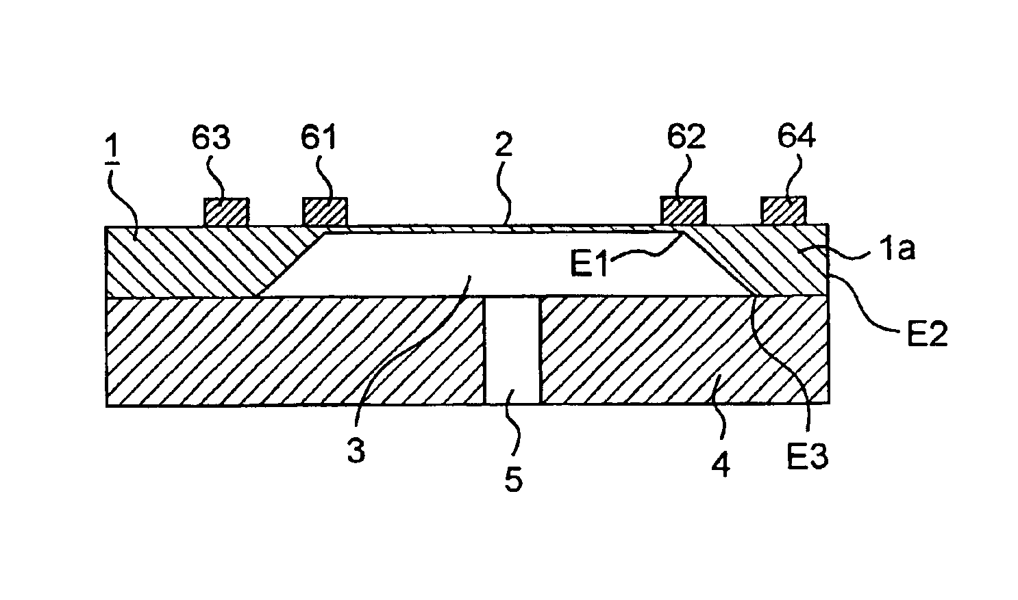
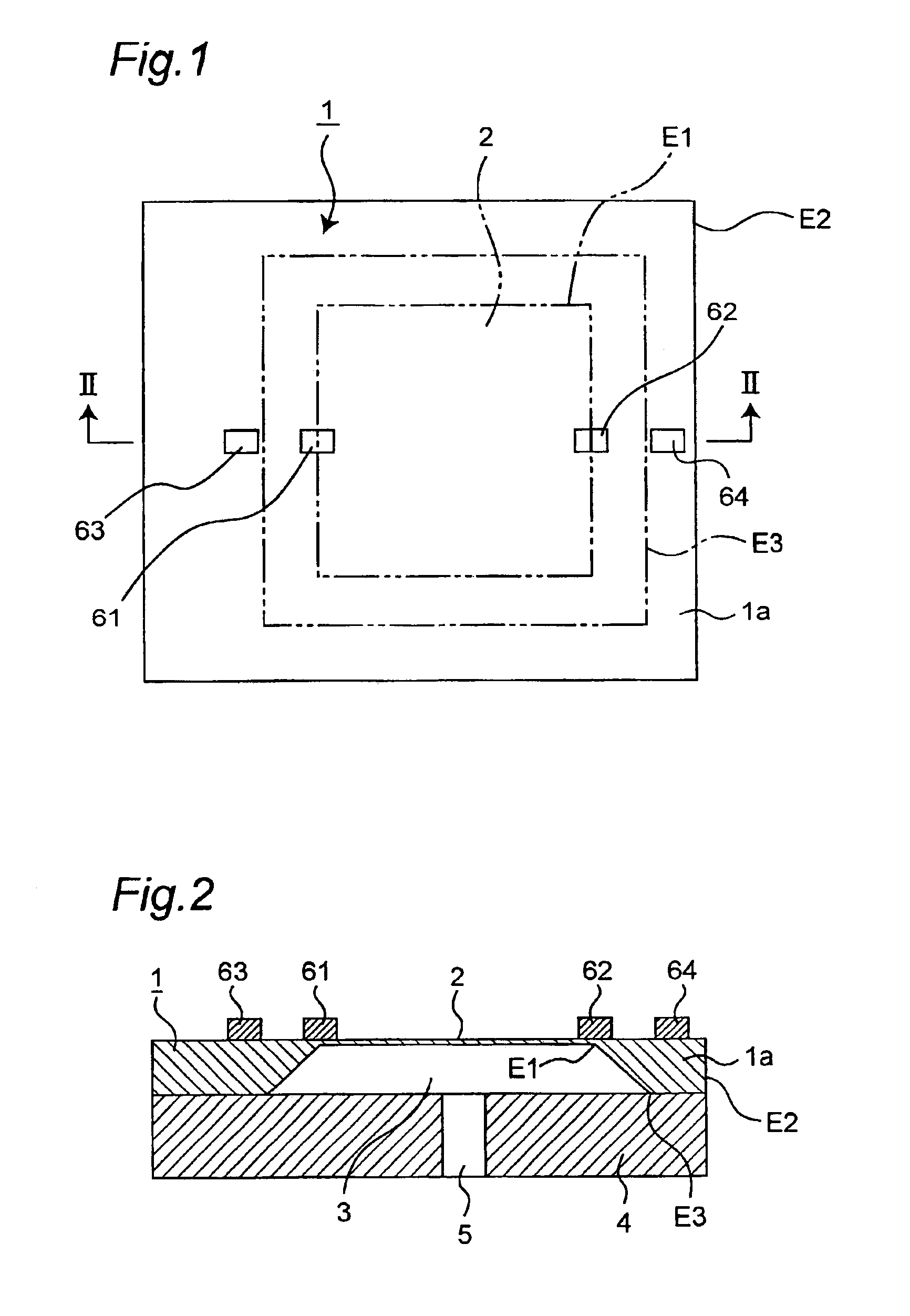
As shown in FIGS. 1 and 2, a mechanical deformation amount sensor according to a first embodiment acts as a pressure sensor for detecting fluid pressure. In this embodiment, a sensor structure 1 is a so-called micro-electro-mechanical systems (MEMS) sensor chip (semiconductor pressure sensor chip) obtained by working a silicon substrate and is constituted by a support portion 1a having a shape of a rectangular frame and a thin-walled diaphragm 2 occupying an inside space of the frame of the support portion 1a. In this pressure sensor chip 1, the diaphragm 2 acting as a thin-walled pressure bearing portion is formed by digging a recess 3 into a portion of a rear face of the pressure sensor chip 1 by anisotropic etching such that a bottom wall of the recess 3, namely, the diaphragm 2 has a predetermined thickness. Thus, as shown in FIG. 1, the support portion 1a has three rectangular frame edges, i.e., an innermost rectangular frame edge E1 bounding the diaphragm 2, an outermost recta...

second embodiment

FIGS. 8 and 9 show a semiconductor pressure sensor according to a second embodiment of the present invention. In the first embodiment, a surface of the pressure sensor chip 1 including the diaphragm 2 is flat and the carbon nanotube resistance elements 61 and 62 are arranged and fixed on this flat surface of the pressure sensor chip 1. The second embodiment is designed to make the best use of such a property of a carbon nanotube that electric resistance of the carbon nanotube changes greatly at its location having a large angle of deformation.

Namely, in this embodiment, a step portion 12 is formed at a boundary of the peripheral edge portion, i.e., a deformation portion of the diaphragm 2 and the support portion 1a as shown in FIG. 9 such that a surface of the diaphragm 2 is set lower than that of the support portion 1a surrounding the diaphragm 2. Each of the carbon nanotube resistance elements 61 and 62 is disposed and fixed so as to longitudinally stride over the step portion 12 ...

third embodiment

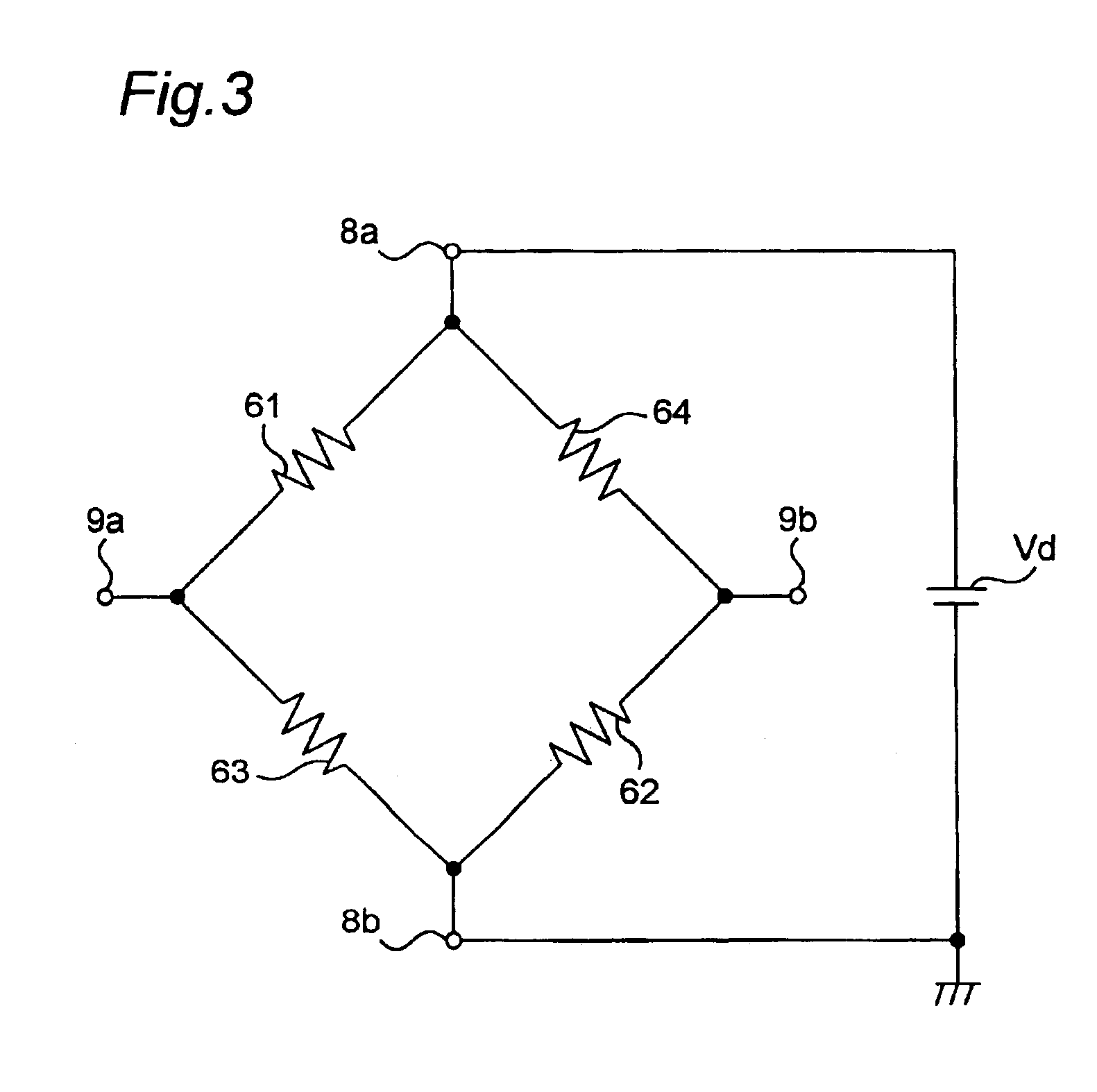
FIGS. 11 and 12 show a semiconductor pressure sensor according to a third embodiment of the present invention. In the first and second embodiments, the bridge circuit is formed by providing the reference resistance elements 63 and 64. In this embodiment, reference resistance elements 63′ and 64′ are provided at a central portion of a surface of the diaphragm 2 such that an axial direction of the reference resistance elements 63′ and 64′ is parallel to that of the carbon nanotube resistance elements 61 and 62 disposed in the peripheral edge portion of the diaphragm 2 and a bridge circuit shown in FIG. 13 is formed by using the reference resistance elements 63′ and 64′. The reference resistance elements 63′ and 64′ are constituted by carbon nanotubes.

In the semiconductor pressure sensor, when fluid pressure is introduced into the recess 3 from the pressure introduction bore 5 of the base 4, a central portion of the diaphragm 2 is deflected by the fluid pressure so as to be expanded up...


PUM

PropertyMeasurementUnit
temperatureaaaaaaaaaa
physicalaaaaaaaaaa
electrical conductivityaaaaaaaaaa

Abstract

A mechanical deformation amount sensor includes a sensor structure which is formed by a semiconductor substrate or an insulating substrate and integrally includes a deformation portion deformable, when a physical quantity to be detected is applied to the sensor structure, due to the physical quantity and a support portion for supporting the deformation portion, a carbon nanotube resistance element which is provided on the deformation portion so as to be mechanically deformed in response to deformation of the deformation portion and a wiring pattern which is formed in a pattern on the sensor structure so as to be connected to the carbon nanotube resistance element. By applying a voltage to the carbon nanotube resistance element via the wiring pattern, a change of electrical conductivity of the carbon nanotube resistance element upon mechanical deformation of the carbon nanotube resistance element is fetched as an electrical signal.

Description

BACKGROUND OF THE INVENTION1. Field of the InventionThe present invention relates to a mechanical deformation amount sensor such as an acceleration sensor, a pressure sensor or the like.2. Description of the Prior ArtAs a sensor for detecting magnitude of a physical quantity to be detected, a mechanical deformation amount sensor is known in which mechanical deformation amount of a sensor structure caused by application of the physical quantity thereto is taken as an index indicative of the magnitude of the physical quantity so as to be converted into an electrical signal. Its typical examples include a semiconductor acceleration sensor and a semiconductor pressure sensor. In the semiconductor acceleration sensor and the semiconductor pressure sensor, the sensor structure is formed by a semiconductor substrate and a phenomenon in which when a stress is applied to a semiconductor crystal, electric resistance of the semiconductor crystal changes, namely, piezoelectric resistance is uti...

Claims


Application Information

Patent Timeline
Patent Type & Authority Patents(United States)
IPC IPC(8): B60J7/04B60J7/057G01L9/00G01P15/12B81B3/00B82B1/00H01L29/84
CPCB81B3/0021B81B3/0086B82Y30/00G01L9/0055G01P15/123B81B2201/0235B81B2201/0257B81B2201/0264Y10S977/956B81B2203/0127B81B2203/0118G01P2015/0828
Inventor MIYAJIMA, HISAKAZUARAKAWA, MASAOYABUTA, AKIRASAKAI, JUN
Owner MATSUSHITA ELECTRIC WORKS LTD
Why Eureka
Try Eureka