Light emitting device and method of manufacturing the same

a technology of light-emitting devices and manufacturing methods, which is applied in the direction of sustainable manufacturing/processing, final product manufacturing, semiconductor/solid-state device details, etc., can solve the problems of short life of light-emitting devices, substrates are likely to be deformed, and plastic films are easily affected by heat, so as to reduce the stress of sealing films. , the effect of preventing a crack on the substra

Inactive Publication Date: 2005-02-01
SEMICON ENERGY LAB CO LTD
View PDF53 Cites 233 Cited by
  • Summary
  • Abstract
  • Description
  • Claims
  • Application Information

AI Technical Summary

Benefits of technology

In view of the above problems, the present invention has an object of providing a light emitting device including an OLED formed on a plastic substrate, which is capable of restraining the degradation due to penetration of moisture or oxygen.
According to the present invention, a plurality of barrier films are laminated. In this manner, even if a crack occurs in one of the barrier films, the other barrier film(s) can effectively prevent moisture or oxygen from penetrating into the organic light emitting layer. Moreover, even though the quality of barrier films is degraded due to a low film formation temperature, a laminate of a plurality of barrier films can effectively prevent moisture or oxygen from penetrating into the organic light emitting layer.
Furthermore, a stress relaxing film, which has a smaller stress than that of the barrier film, is sandwiched between the barrier films to reduce the entire stress of the is sealing film. Thus, a crack due to stress hardly occurs in a multi-layered barrier film, in which a stress relaxing film is interposed between barrier films, as compared with a single-layered barrier film having the same thickness.
Accordingly, a multi-layered barrier film can effectively prevent moisture or oxygen from penetrating into the organic light emitting layer as compared with a single-layered barrier film having the same thickness. In addition, a crack due to stress hardly occurs in such a multi-layered barrier film.
Moreover, a laminate structure of barrier films and a stress relaxing film provides a further flexibility to a device, thereby preventing a crack upon bend of the substrate.
Furthermore, according to the present invention, a film for sealing an OLED formed on a substrate (hereinafter, referred to as a sealing film) may also have the above-mentioned multi-layered structure. With such a structure, moisture or oxygen can be effectively prevented from penetrating into the organic light emitting layer. In addition, a crack is prevented from occurring upon bend of the substrate. As a result, a light emitting device having enhanced flexibility can be realized.

Problems solved by technology

Since the degradation of an organic light emitting layer is accelerated by moisture and oxygen, the lifetime of a light emitting device tends to be short by the penetration of moisture or oxygen.
In general, however, a substrate such as a plastic film is easily affected by heat.
At an excessively elevated film formation temperature for an insulating film such as a silicon nitride film or a silicon oxynitride film, a substrate is likely to be deformed.
On the contrary, at an excessively low film formation temperature, the quality of a film may be degraded, making it difficult to sufficiently prevent the penetration of moisture or oxygen.
Furthermore, if a thickness of an insulating film such as a silicon nitride film or a silicon oxynitride film is increased so as to prevent the penetration of moisture or oxygen, a stress is correspondingly increased to easily cause a crack in the film.
Moreover, with an increase in thickness, a crack is likely to be generated in the insulating film when the substrate is bent.

Method used


Image

  • Light emitting device and method of manufacturing the same
  • Light emitting device and method of manufacturing the same
  • Light emitting device and method of manufacturing the same

Examples


embodiment mode 1

(Embodiment Mode 1)

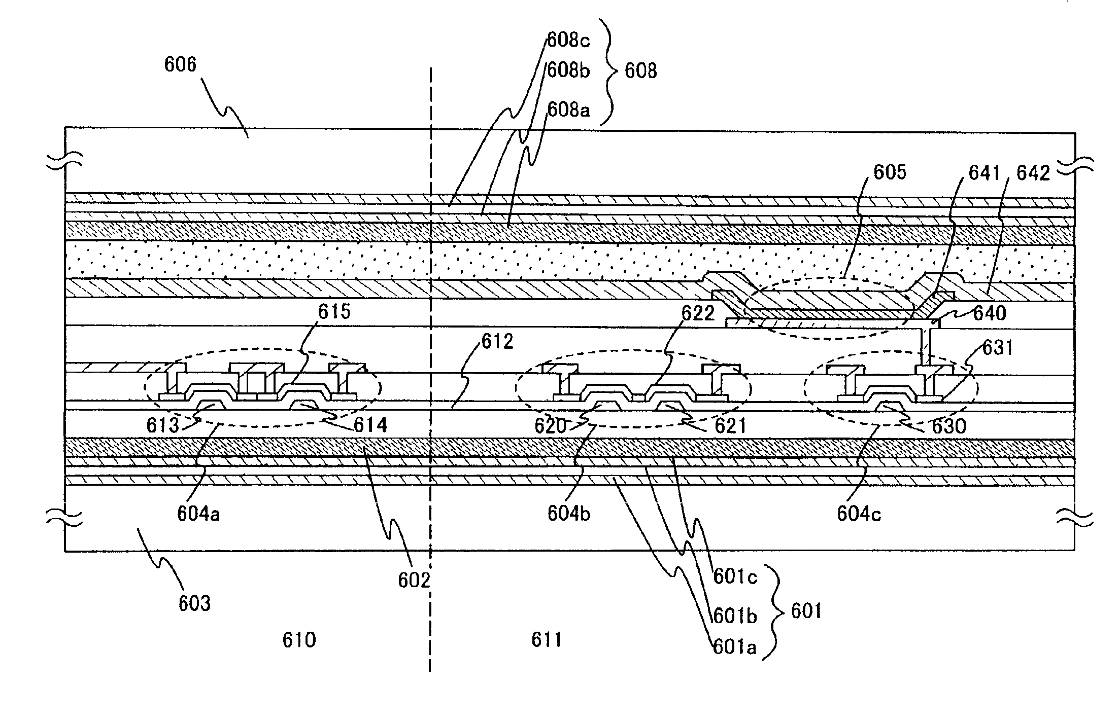
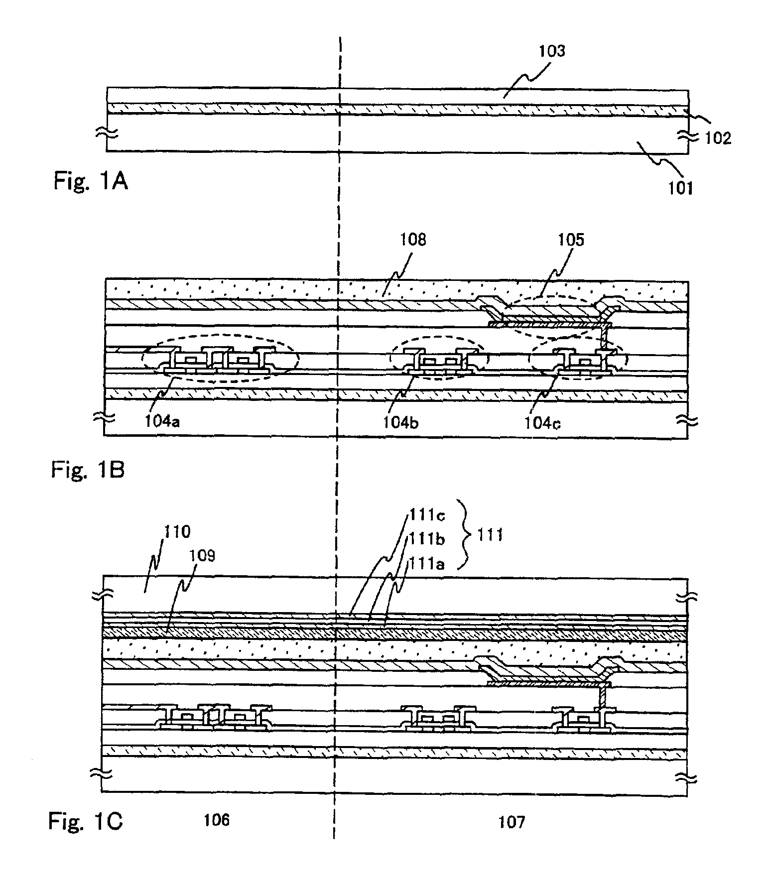
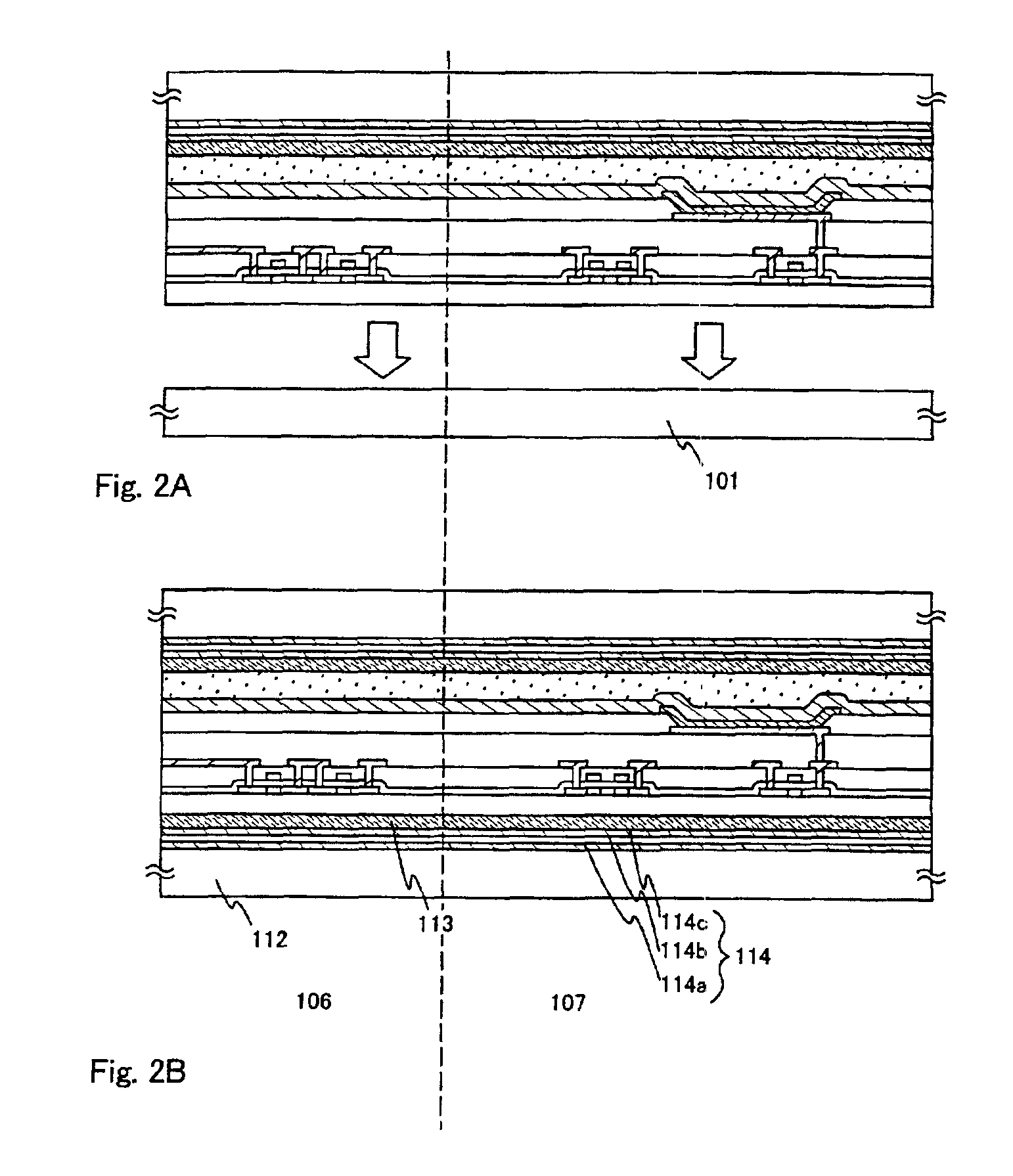
In FIG. 1A, a first bonding layer 102 made of an amorphous silicon film is formed to have a thickness of 100 to 500 nm (300 nm in this embodiment mode) on a first substrate 101. Although a glass substrate is used as the first substrate 101 in this embodiment mode, a quartz substrate, a silicon substrate, a metal substrate or a ceramic substrate may be alternatively used. Any material can be used for the first substrate 101 as long as it is resistant to a treatment temperature in the later manufacturing steps.

As a method of forming the first bonding layer 102, a low pressure thermal CVD method, a plasma CVD method, a sputtering method or an evaporation method may be used. On the first bonding layer 102, an insulating film 103 made of a silicon oxide film is formed to have a thickness of 200 nm. As a method of forming the insulating film 103, a low pressure thermal CVD method, a plasma CVD method, a sputtering method or an evaporation method may be used. The insulat...

embodiment mode 2

(Embodiment Mode 2)

Next, another embodiment mode of the present invention, which differs from the above-described first embodiment mode, will be described.

In FIG. 3A, a first bonding layer 202 made of an amorphous silicon film is formed to have a thickness of 100 to 500 nm (300 nm in this embodiment mode) is formed on a first substrate 201. Although a glass substrate is used as the first substrate 201 in this embodiment mode, a quartz substrate, a silicon substrate, a metal substrate or a ceramic substrate may be alternatively used. Any material can be used for the first substrate 201 as long as it is resistant to a treatment temperature in the later manufacture steps.

As a method of forming the first bonding layer 202, a low pressure thermal CVD method, a plasma CVD method, a sputtering method or an evaporation method may be used. On the first bonding layer 202, an insulating film 203 made of a silicon oxide film is formed to have a thickness of 200 nm. As a method of forming the in...

embodiment 1

(Embodiment 1)

In Embodiment 1, the outward appearance of a light emitting device according to the present invention and its connection to an FPC will be described.

FIG. 5A shows an example of a top view of a light emitting device according to the present invention, described in Embodiment mode 1. A second substrate 301 and a third substrate 302 are both plastic substrates having flexibility. A pixel portion 303 and driving circuits (a source-side driving circuit 304 and a gate-side driving circuit 305) are provided between the second substrate 301 and the third substrate 302.

In FIG. 5A, there is shown an example where the source-side driving circuit 304 and the gate side-driving circuit 305 are formed on the substrate on which the pixel portion 303 is also formed. However, the driving circuits represented by the source-side driving circuit 304 and the gate side-driving circuit 305 may be formed on a different substrate from the substrate on which the pixel portion 303 is formed. In t...


PUM


Abstract

The present invention has an object of providing a light emitting device including an OLED formed on a plastic substrate, which can prevent the degradation due to penetration of moisture or oxygen. On a plastic substrate, a plurality of films for preventing oxygen or moisture from penetrating into an organic light emitting layer in the OLED (hereinafter, referred to as barrier films) and a film having a smaller stress than that of the barrier films (hereinafter, referred to as a stress relaxing film), the film being interposed between the barrier films, are provided. Owing to a laminate structure of a plurality of barrier films, even if a crack occurs in one of the barrier films, the other barrier film(s) can effectively prevent moisture or oxygen from penetrating into the organic light emitting layer. Moreover, the stress relaxing film, which has a smaller stress than that of the barrier films, is interposed between the barrier films, thereby making it possible to reduce a stress of the entire sealing film. As a result, a crack due to stress hardly occurs.

Description

BACKGROUND OF THE INVENTION1. Field of the InventionThe present invention relates to a method of manufacturing a semiconductor device, more specifically, to a light emitting device including a light emitting element, for example, an organic light emitting diode (OLED), formed on a plastic substrate. The present invention also relates to an OLED module in which an IC including a controller and the like is mounted onto an OLED panel. Throughout the specification, OLED panels and OLED modules are generically referred to as light emitting devices. The present invention further relates to an electrical appliance using the light emitting device.2. Description of the Related ArtRecently, a technique for forming a TFT (thin film transistor) on a substrate has been remarkably developed, and continues to be further developed for its application to active matrix display devices. Particularly, a TFT using a polysilicon film can operate at a high speed because such a TFT has a higher field effec...

Claims


Application Information

Patent Timeline
Patent Type & Authority Patents(United States)
IPC IPC(8): H01L51/50H01L51/52H01L27/32H01L27/28H05B33/00
CPCH01L27/3244H01L51/5237H01L51/529H01L51/56H01L51/5253H01L27/326H01L51/0097H01L2221/68368H01L2227/326H01L2251/5338H01L2251/5315Y02E10/549Y02P70/50H10K59/12H10K59/121H10K77/111H10K50/844H10K50/8445H10K50/87H10K71/80H10K59/1201H10K2102/3026H10K2102/311H10K71/00H05B33/00H10K50/84
Inventor YAMAZAKI, SHUNPEITAKAYAMA, TORUAKIBA, MAI
Owner SEMICON ENERGY LAB CO LTD
Why Eureka
Try Eureka