Group-III nitride based high electron mobility transistor (HEMT) with barrier/spacer layer

a high electron mobility, transistor technology, applied in the direction of basic electric elements, electrical apparatus, semiconductor devices, etc., can solve the problems of low electron mobility, general limited mobility of 2deg, and degrade the high performance gain of si based hemt, so as to reduce piezoelectric scattering, keep the hemt gate leakage low, and high piezoelectric charge

Inactive Publication Date: 2005-02-01
CREE INC +1
View PDF5 Cites 343 Cited by
  • Summary
  • Abstract
  • Description
  • Claims
  • Application Information

AI Technical Summary

Benefits of technology

The HEMT's AlyGa1−yN layer on the GaN layer provides a high piezoelectric charge and a reduction in piezoelectric scattering at the interface between the two layers. The AlyGa1

Problems solved by technology

One disadvantage of Si is that it has low electron mobility (approximately 1450 cm2/V-s), which produces a high source resistance.
This resistance can degrade the Si based HEMT's high performance gain.
However, GaAs has a relatively small bandgap (1.42 eV at room temperature) and relatively small breakdown voltage, which prevents GaAs based HEMTs from providing high power at high frequencies.
However, the 2DEG's mobility is generally limited by the interface roughness and piezoelectric scattering at the interface between the GaN and Al

Method used


Image

  • Group-III nitride based high electron mobility transistor (HEMT) with barrier/spacer layer
  • Group-III nitride based high electron mobility transistor (HEMT) with barrier/spacer layer
  • Group-III nitride based high electron mobility transistor (HEMT) with barrier/spacer layer

Examples


Embodiment Construction

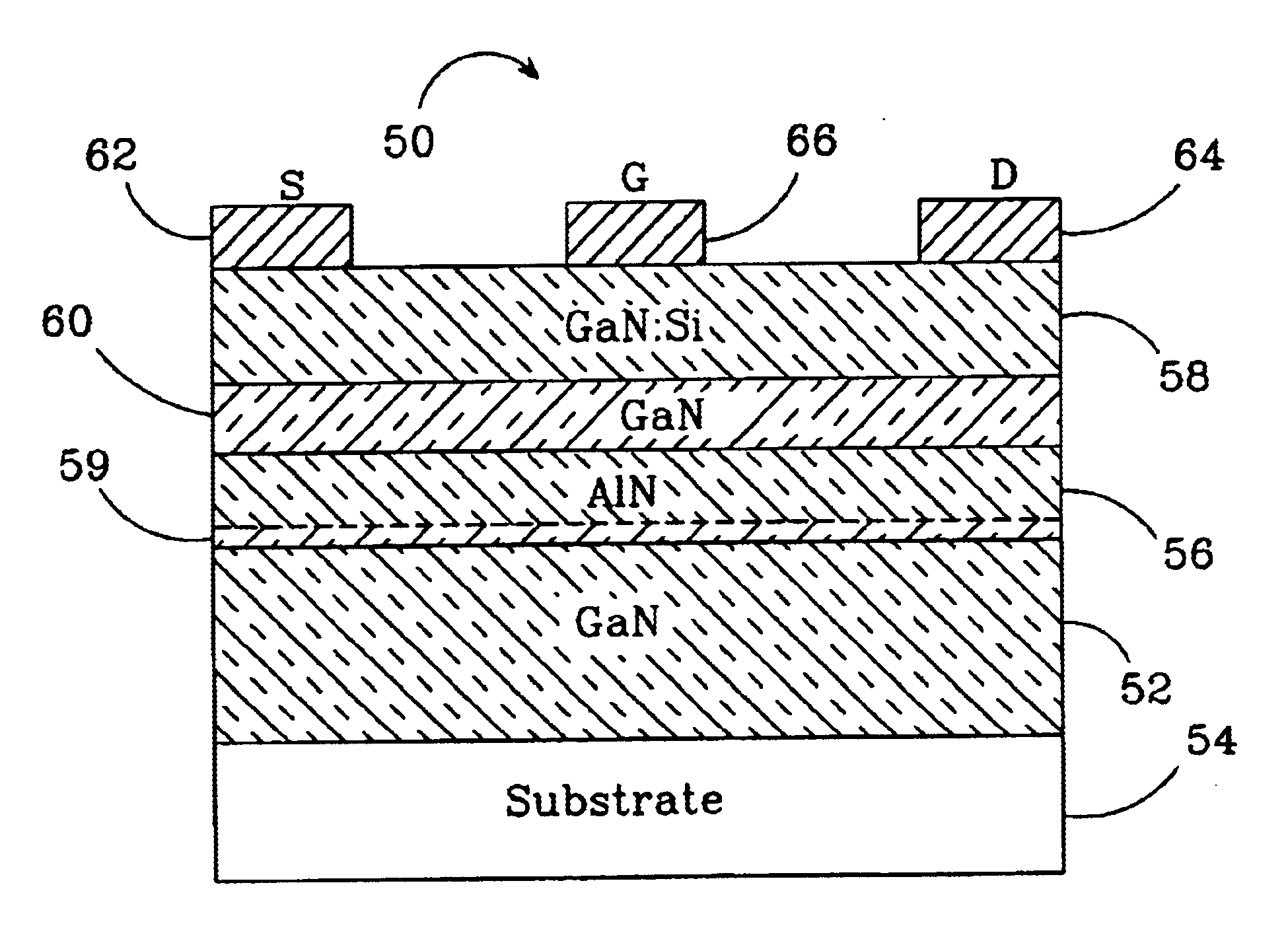
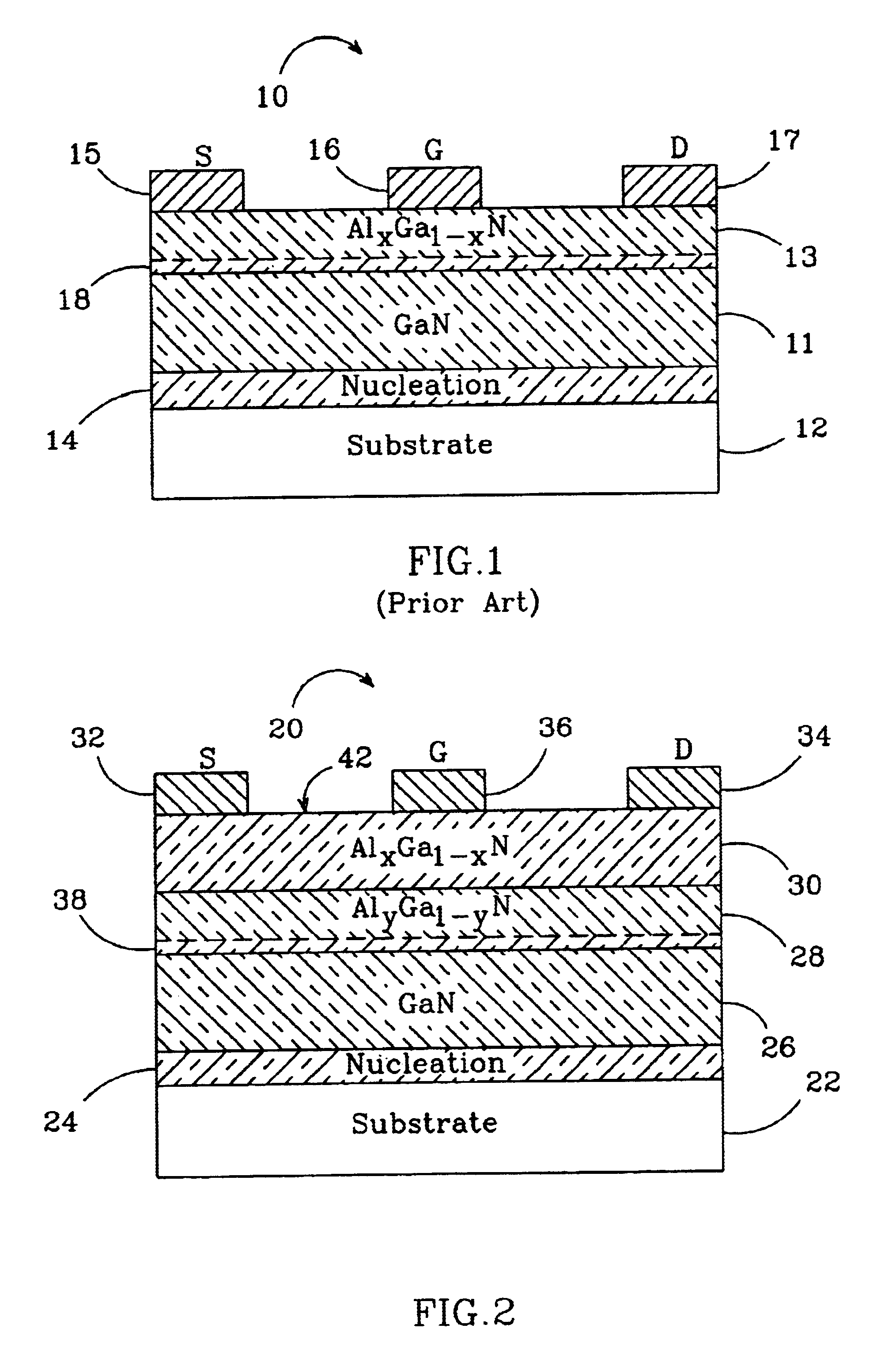
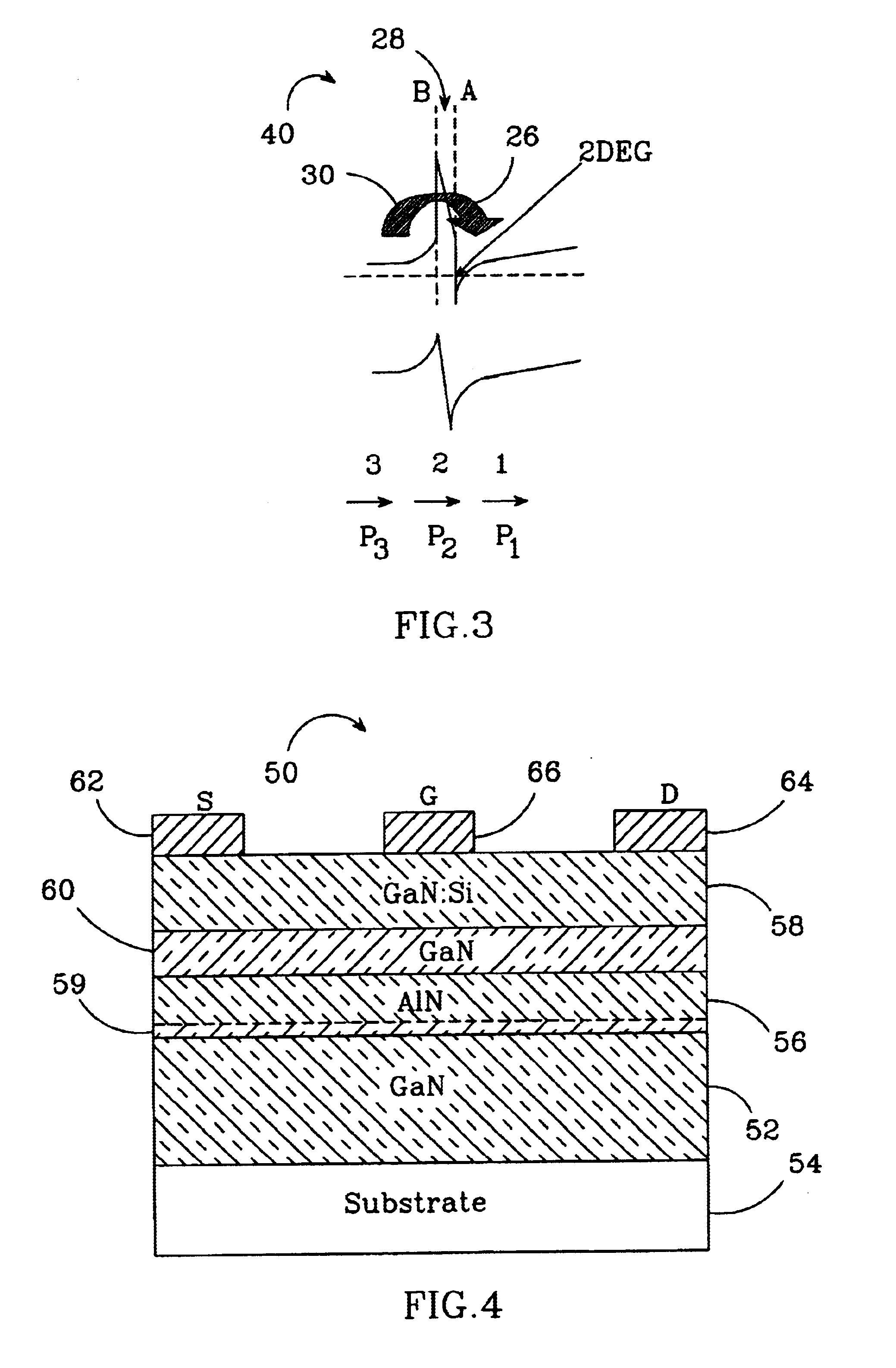
FIG. 2 shows one embodiment of a HEMT 20 constructed in accordance with the present invention. It comprises a substrate 22 that can be made of different materials such as sapphire (Al2O3), silicon carbide (SiC), gallium nitride (GaN), or silicon (Si). The preferred substrate is a 4H polytype of silicon carbide. Other silicon carbide polytypes can also be used including 3C, 6H and 15R polytypes.

Silicon carbide has a much closer crystal lattice match to Group III nitrides than sapphire and results in Group III nitride films of higher quality. Silicon carbide also has a very high thermal conductivity so that the total output power of Group III nitride devices on silicon carbide is not limited by the thermal dissipation of the substrate (as may be the case with some devices formed on sapphire). Also, the availability of silicon carbide substrates provides the capacity for device isolation and reduced parasitic capacitance that make commercial devices possible. SiC substrates are availab...


PUM


Abstract

A Group III nitride based high electron mobility transistors (HEMT) is disclosed that provides improved high frequency performance. One embodiment of the HEMT comprises a GaN buffer layer, with an AlyGa1−yN (y=1 or y 1) layer on the GaN buffer layer. An AlxGa1−xN (0≦x≦0.5) barrier layer on to the AlyGa1−yN layer, opposite the GaN buffer layer, AlyGa1−yN layer having a higher Al concentration than that of the AlxGa1−xN barrier layer. A preferred AlyGa1−yN layer has y=1 or y˜1 and a preferred AlxGa1−xN barrier layer has 0≦x≦0.5. A 2DEG forms at the interface between the GaN buffer layer and the AlyGa1−yN layer. Respective source, drain and gate contacts are formed on the AlxGa1−xN barrier layer. The HEMT can also comprising a substrate adjacent to the buffer layer, opposite the AlyGa1−yN layer and a nucleation layer between the AlxGa1−xN buffer layer and the substrate.

Description

BACKGROUND OF THE INVENTION1. Field of the InventionThis invention relates to high frequency solid state transistors, and more particularly to Group-III nitride based high electron mobility transistors (HEMTs).2. Description of the Related ArtHEMTs are a common type of solid state transistor that are regularly fabricated from semiconductor materials such as Silicon (Si) or Gallium Arsenide (GaAs). One disadvantage of Si is that it has low electron mobility (approximately 1450 cm2 / V-s), which produces a high source resistance. This resistance can degrade the Si based HEMT's high performance gain. [CRC Press, The Electrical Engineering Handbook, Second Edition, Dorf, p.994, (1997)]GaAs based HEMTs have become the standard for signal amplification in civil and military radar, handset cellular, and satellite communications. GaAs has a higher electron mobility (approximately 6000 cm2 / V-s) and a lower source resistance than Si, which allows GaAs based devices to function at higher frequen...

Claims


Application Information

Patent Timeline
IPC IPC(8): H01L29/778H01L29/66H01L29/02H01L29/20H01L29/812H01L21/338
CPCH01L29/7783H01L29/2003H01L29/778
Inventor CHAVARKAR, PRASHANTSMORCHKOVA, IOULIA P.KELLER, STACIAMISHRA, UMESHWALUKIEWICZ, WLADYSLAWWU, YIFENG
Owner CREE INC
Why Eureka
Try Eureka