Method of producing a semiconductor integrated circuit device and the semiconductor integrated circuit device

a technology of integrated circuits and semiconductors, applied in semiconductor devices, semiconductor/solid-state device details, electrical apparatus, etc., can solve the problems of preventing the cutting of substrates, causing voids to be generated in silicon oxide films, and causing short circuits in adjacent contact holes

Inactive Publication Date: 2005-02-01
RENESAS ELECTRONICS CORP
View PDF19 Cites 3 Cited by
  • Summary
  • Abstract
  • Description
  • Claims
  • Application Information

AI Technical Summary

Benefits of technology

[0028]According to the invention, the etching conditions are changed in the midway of the formation in forming the second hole part reaching the semiconductor substrate by etching. Therefore, the semiconductor substrate underlying the bottom of the second hole part can be prevented from being cut.
[0029]Additionally, according to the invention, the semiconductor substrate can be prevented from being cut by etching in forming the second hole part reaching the semiconductor substrate. Therefore, a damaged layer due to etching can be prevented from generating in the semiconductor substrate.
[0030]Furthermore, according to the invention, an insulating film having a main component of silicon oxide can be prevented from being exposed in the sidewalls of the second hole part reaching the semiconductor substrate. Thus, the insulating film can be prevented from being wet etched by the cleaning process.
[0031]Moreover, according to the invention, the insulating film having a main component of silicon oxide can be prevented from being wet etched from the sidewalls of the second hole part. Therefore, the adjacent second hole parts can be prevented from being short-circuited.

Problems solved by technology

However, the inventors found the following problems in the Self Align (SAC) technique described above.
More specifically, as an aspect ratio (a ratio between a space height and a space width) of the space between the gate electrodes is increased, voids tend to be generated in the silicon oxide film burying the space.
However, these films are liable to wet etching and thus voids might be generated due to the cleaning process after forming the contact holes.
When the voids are generated, a problem arises that the adjacent contact holes are short-circuited by a conductive film through the voids when the contact holes are buried with a conductive film such as a polycrystalline silicon film after forming the contact holes.

Method used


Image

  • Method of producing a semiconductor integrated circuit device and the semiconductor integrated circuit device
  • Method of producing a semiconductor integrated circuit device and the semiconductor integrated circuit device
  • Method of producing a semiconductor integrated circuit device and the semiconductor integrated circuit device

Examples


embodiment 1

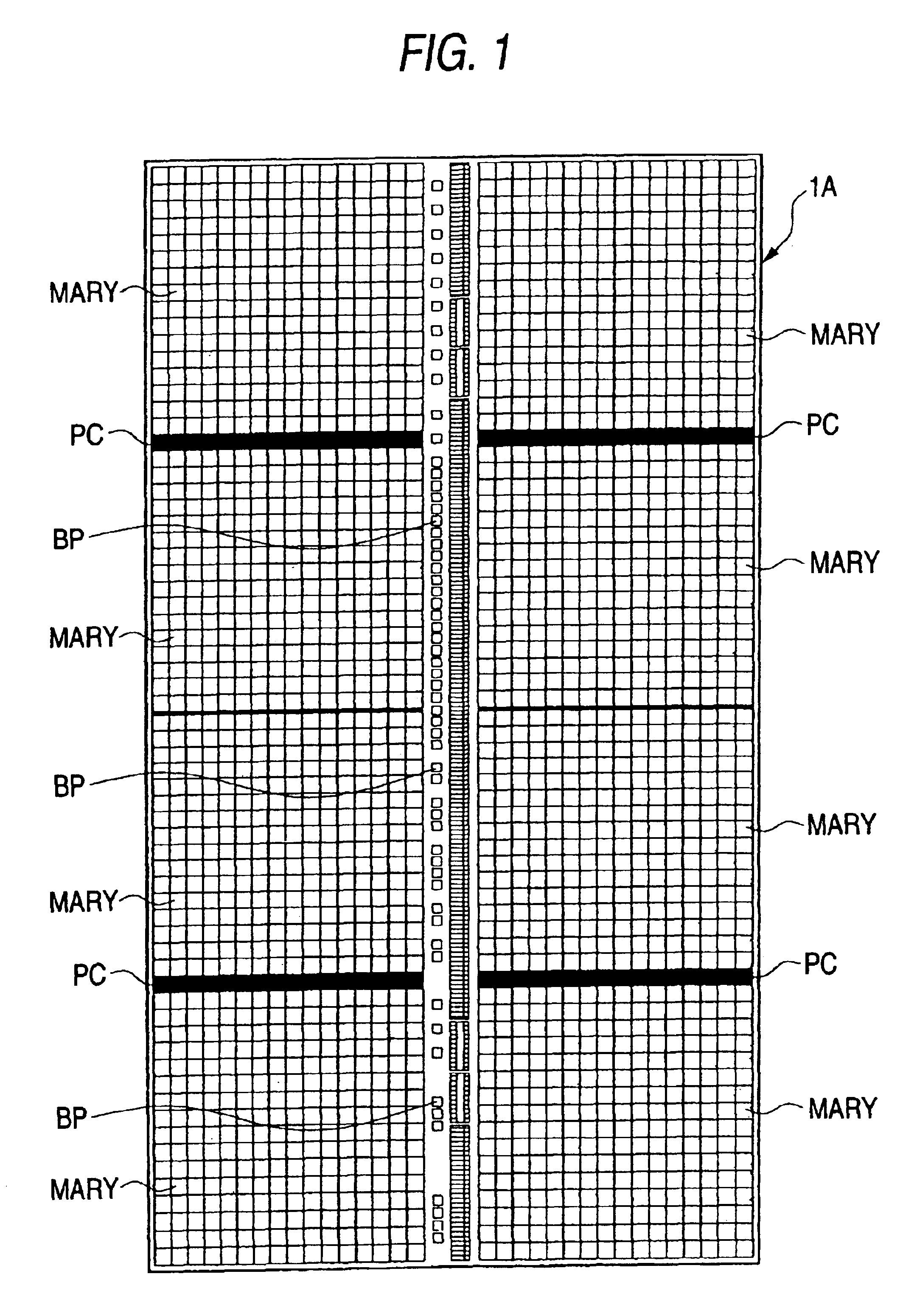
[0121]FIG. 1 depicts a whole plan view illustrating a semiconductor chip 1A formed with a DRAM (Dynamic Random Access Memory) of

[0122]On a main surface of the rectangular semiconductor chip 1A is formed a DRAM having 256 Mbits of storage capacity, for example. This DRAM has a storage part comprised of a plurality of memory arrays (MARY) and a peripheral circuit part PC disposed therearound. Additionally, in the center part of the semiconductor chip 1A, a plurality of bonding pads BP to which a wire or bump electrode is connected are arranged in a row.

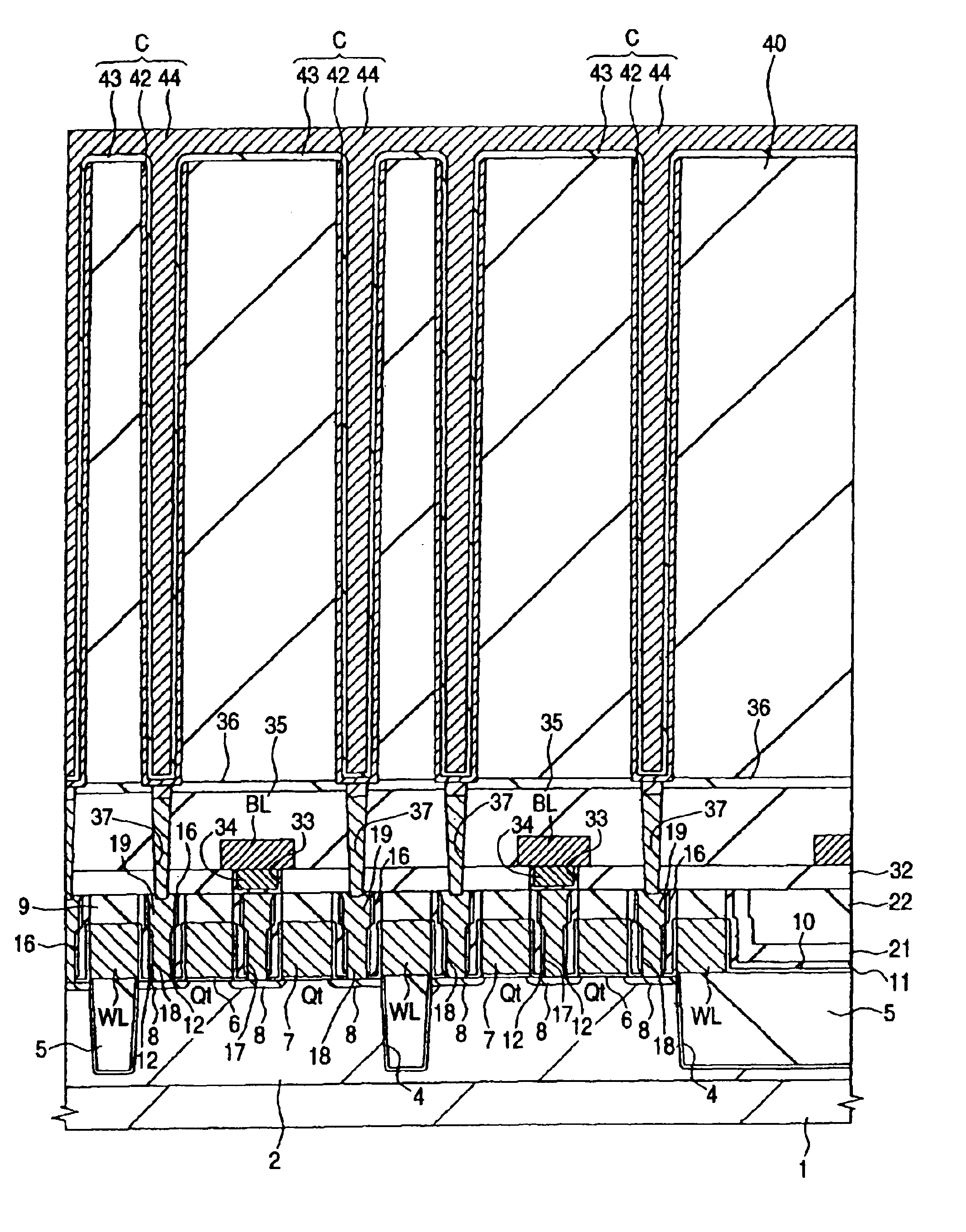
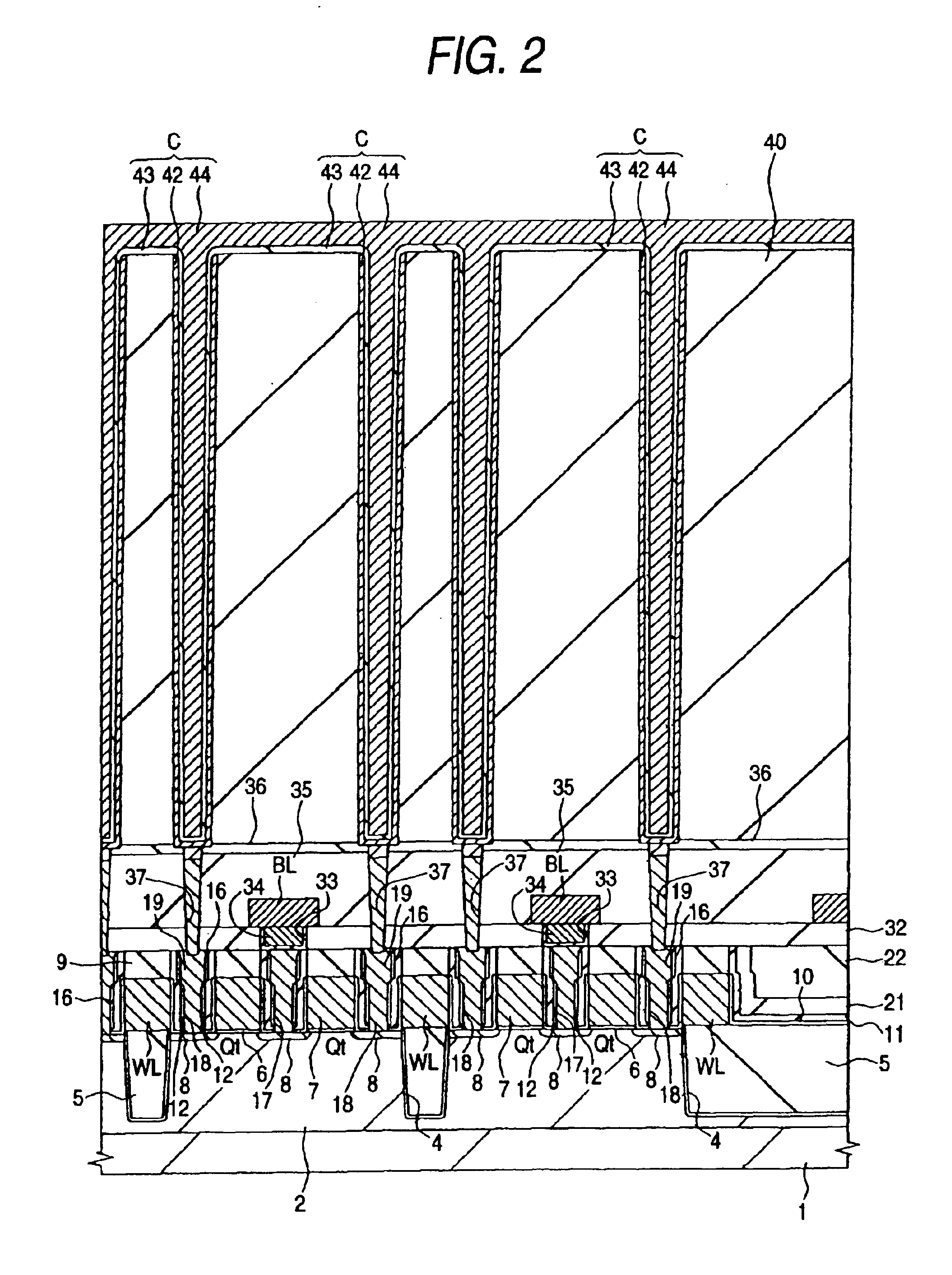
[0123]FIG. 2 depicts a section of a principal part of a semiconductor substrate illustrating one end part of the storage part described above.

[0124]For example, or the main surface of the semiconductor substrate 1 comprised of p-type single crystal silicon are formed a p-type well 2, and or the p-type well 2 is formed a device isolation trench 4. On an active region of the p-type well 2 whose periphery is defined by the device isolation...

embodiment 2

[0187]Next, the method for fabricating the DRAM of the embodiment 2 will be described in accordance with FIGS. 60 to 65.

[0188]The method for fabricating the DRAM of the embodiment 2 is the same until the processes described with reference to FIGS. 3 to 21 in the embodiment 1.

[0189]After that, as shown in FIGS. 60 and 61, the insulating film 11 in the bottom of the hole parts 13 and 14 is removed by anisotropic etching (dry etching). At this time, a mixed gas of CHF3 and O2 is used as an etching gas to increase the etching selective ratio of the insulating film 11 comprised of the silicon nitride film with respect to the insulating film 10 comprised of the silicon oxide film. Consequently, the insulating film 11 in the bottom of the hole parts 13 and 14 can be etched, using the insulating film 10 as an etching stopper.

[0190]As described above, the insulating film 11 in the bottom of the hole parts 13 and 14 can be etched using the insulating film 10 as an etching stopper. Thereby, th...

embodiment 3

[0198]Next, the method for fabricating the DRAM of the embodiment 3 will be described in accordance with FIGS. 66 to 73.

[0199]The method for fabricating the DRAM of the embodiment 3 is the same until the processes described with reference to FIGS. 3 to 23 in the embodiment 1 or the processes described with reference to FIGS. 60 to 65 in the embodiment 2. However, a deposited amount of the silicon nitride film configuring the insulating film 11 (third insulating film) is set about 10 nm.

[0200]Then, as shown in FIGS. 66 to 69 or 70 to 73, a silicon oxide film having a film thickness not completely burying the space between the gate electrodes 7 (word lines WL) is deposited over the semiconductor substrate 1 including the inside of the hole parts 13 and 14 to form an insulating film 12A (fifth insulating film). In the embodiment 3, the insulating film 12A is formed by CVD and the film thickness thereof can be formed to be about 30 nm, for example. The silicon oxide film configuring the...


PUM


Abstract

An amount of a semiconductor substrate cut due to etching in the bottom of a contact hole formed by the SAC technique is reduced. Silicon oxide films are dry etched under the conditions of increasing the etching selective ratio of the silicon oxide films to an insulating film. Then, the conditions are changed to those increasing the etching selective ratio of the insulating film to the silicon oxide films and the insulating film is etched by a predetermined amount.

Description

CROSS-REFERENCE TO RELATED APPLICATIONS[0002]This application is a continuation of application Ser. No. 10 / 256,027 filed Sep. 27, 2002, now abandoned, which is a division of application Ser. No. 10 / 036,449 filed Jan. 7, 2002 (now U.S. Pat. No. 6,482,727).BACKGROUND OF THE INVENTION[0003]The present invention relates to a method of producing a semiconductor integrated circuit device and a semiconductor integrated circuit device, particularly to an effective technique adapted to manufacture of a semiconductor integrated circuit device having a DRAM (Dynamic Random Access Memory).[0004]In a recent large DRAM of 64 or 256 megabits (Mbits), in forming a contact hole for connecting a bit line or information storage capacitive element to a semiconductor substrate in a space between gate electrodes of a miniaturized memory cell selecting MISFET, the top and sidewalls of the gate electrodes are covered with a silicon nitride film, a silicon oxide film burying the space between the gate elect...

Claims


Application Information

Patent Timeline
Patent Type & Authority Patents(United States)
IPC IPC(8): H01L21/60H01L21/02H01L21/70H01L21/8242H01L21/302H01L21/28H01L21/3065H01L27/108
CPCH01L21/76831H01L21/76897H01L27/10873H01L27/10888H01L27/10855H10B12/05H10B12/485H10B12/0335H01L21/28
Inventor ENOMOTO, HIROYUKIMARUYAMA, HIROYUKIYOSHIDA, MAKOTO
Owner RENESAS ELECTRONICS CORP
Why Eureka
Try Eureka