Method of manufacturing semiconductor device

a manufacturing method and technology of semiconductors, applied in semiconductor/solid-state device manufacturing, basic electric elements, electric devices, etc., can solve the problems of oozing out of metal, hygroscopic, and easy plasma damage of low-permittivity films, and achieve enhanced adhesion between seal layers and insulation films, enhanced density, and recovery of silicon (si) dangling bonds

Inactive Publication Date: 2010-01-19
SONY CORP
View PDF9 Cites 1 Cited by
  • Summary
  • Abstract
  • Description
  • Claims
  • Application Information

AI Technical Summary

Benefits of technology

[0023]Thus, there is a need to reduce the defects in reliability, without causing an increase in via resistance, by using a seal layer for restraining influences of plasma damages.
[0025]According to the first embodiment of the present invention, the EB-cure or UV-cure is applied to the seal layer, so that the number of silicon-oxygen-silicon (Si—O—Si) linkage components is increased as compared with the crosslinking reaction, and the adhesion between the seal layer and the insulation film is enhanced even if the insulation film is a low-permittivity (low-k) film. In addition, recovery of silicon (Si) dangling bonds in the insulation film by carbon (alkyl groups) is accelerated. Furthermore, enhancement of denseness of the film is accelerated by recombination.
[0026]According to the first embodiment of the present invention, enhancement of denseness of the seal layer, improvement of the adhesion, and recovery of the damaged layers in the low-permittivity (low-k) film are realized, so that the sealing performance of the seal layer can be enhanced. Therefore, even in the case where the seal layer is formed to have an extremely small thickness (for example, 0.5 nm or below) such that the rise in resistance at the bottom part of a via will not matter, deterioration of film quality of the barrier layer formed in a recess in a insulation film due to oozing-out of moisture from the inside of the insulation film is restrained. In addition, oozing-out of metal into the insulation film, a rise in the resistance at the via, and such defects as stress migration and electro-migration arising from the via can be obviated, whereby enhanced reliability is promised.

Problems solved by technology

In general, a low-permittivity film is susceptible to plasma damages at the time of processing thereof, and, as a result, tends to be hygroscopic.
Where absorption of moisture into the insulation film has occurred, corrosion (e.g., oxidation) of the barrier metal film is caused upon degassing, resulting in oozing out of the metal into the insulation film or an increase in the via resistance due to deterioration of the barrier property.
In addition, the adhesion between the insulation film and the copper seed layer is also deteriorated, generating such fatal defects as electro-migration and stress migration arising from the vias.
However, this process has the problem that the bottom parts of the vias cannot be sealed, and the problem that the bottom parts of the vias undergo etching damages during the spacer forming process, resulting in a rise in the interlayer capacity (refer to Non-patent Document 2 (S. Arakawa, I. Mizuno, Y. Ohoka, K. Nagahata, K. Tabuchi, R. Kanamura and S. Kadomura, “Breakthrough Integration of 32 nm-mode Cu / Ultra Low-k SiOC (k=2.0) Interconnects by using Advanced Pore-Sealing and Low-k Hard Mask Technologies”, 2006 IEEE p210-212, 2004.)).
These problems become more conspicuous as the lowering in the permittivity of the insulation film is accelerated.
In this case, however, the coverage of the side wall parts would be insufficient, and the sealing effect would be deficient, resulting in deteriorated reliability.
This is not permissible on a device design basis.
Besides, in the case where the thickness of the seal layer 215 is 0.5 nm, defects are generated upon the subsequent test of reliability (stress migration, electro-migration).

Method used


Image

  • Method of manufacturing semiconductor device
  • Method of manufacturing semiconductor device
  • Method of manufacturing semiconductor device

Examples


first embodiment

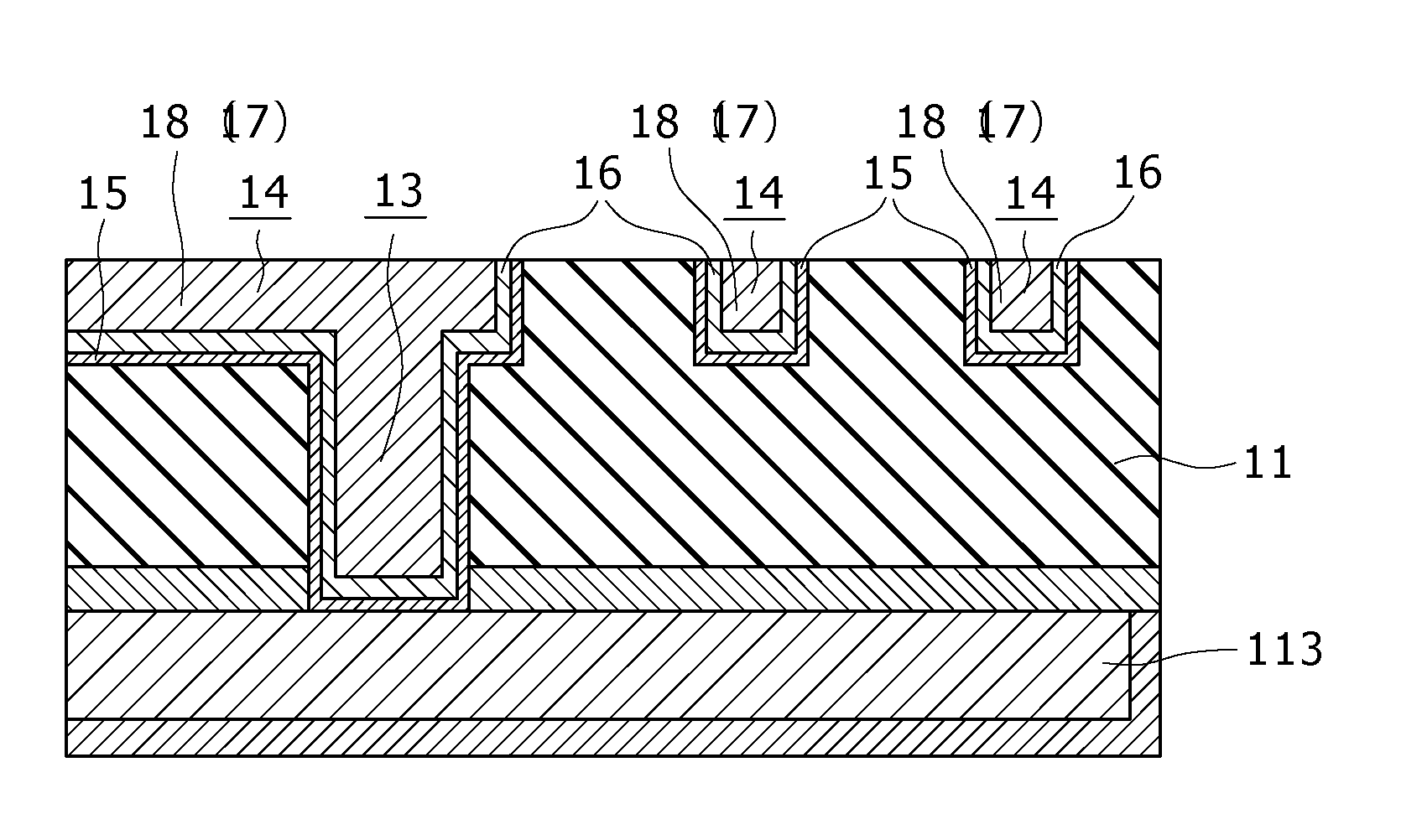
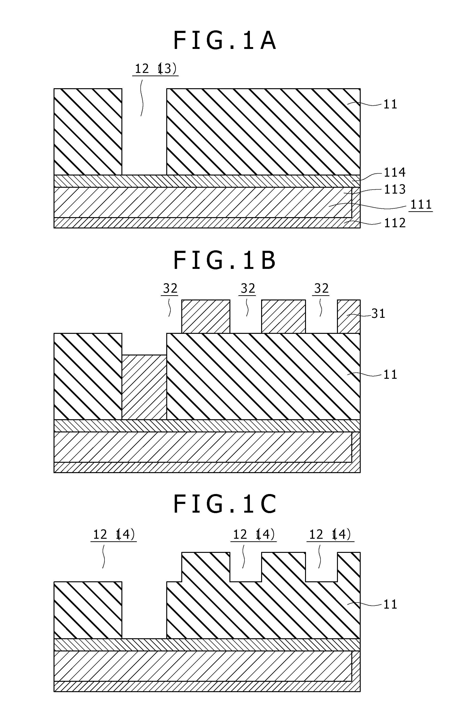
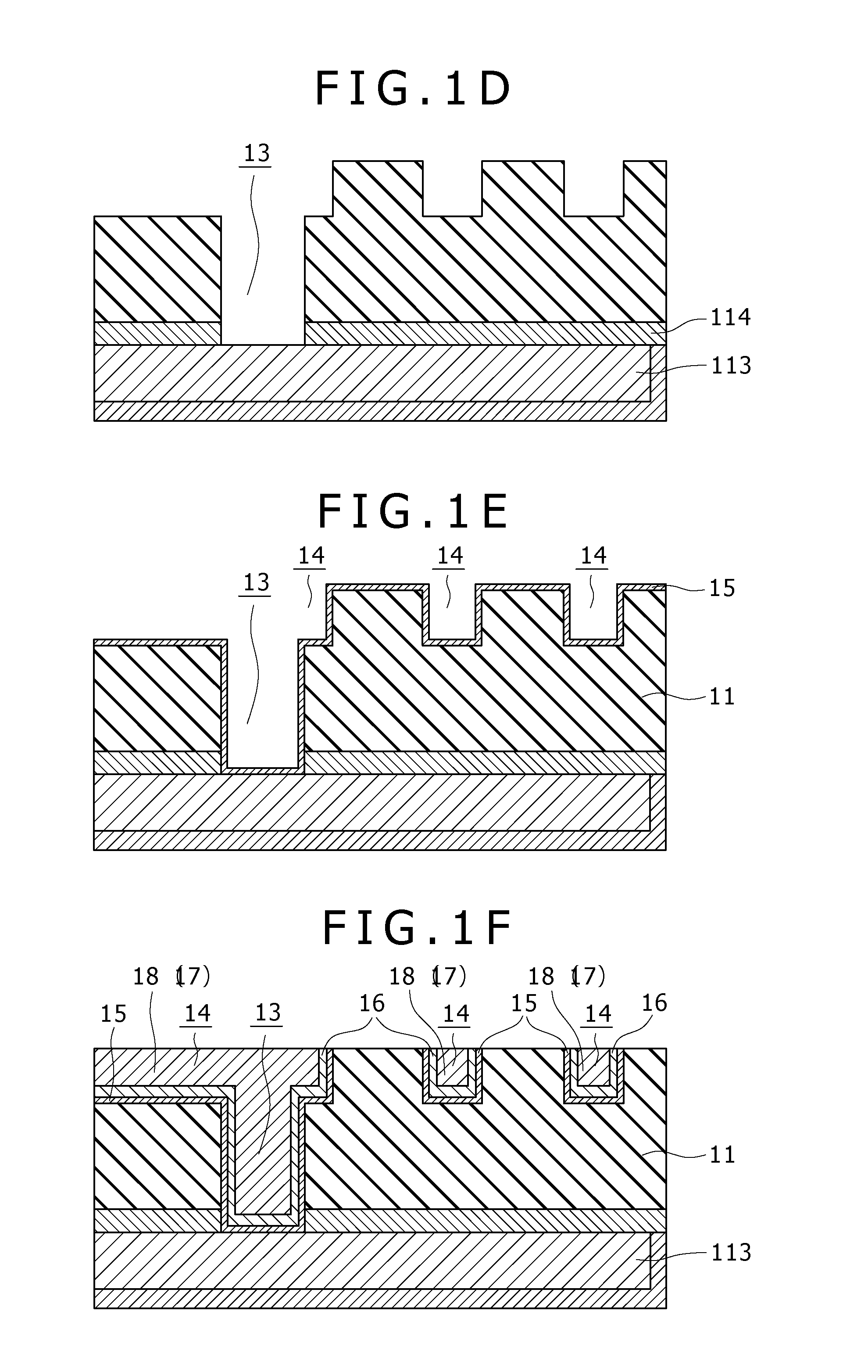
[0040]Now, the method of manufacturing a semiconductor device in the present invention will be described below, referring to manufacturing step sectional views shown in FIGS. 1A to 1F.

[0041]As shown in FIG. 1A, a wiring groove 111 is formed in an insulating film (not shown) formed on a semiconductor substrate (not shown), and a wiring 113 is formed in the inside of the wiring groove 111, with a barrier metal layer 112 therebetween. The wiring 113 is formed from copper in a thickness of 60 nm. Next, a barrier layer 114 covering the wiring 113 is formed. The barrier layer 114 includes a silicon carbonitride (SiCN) film formed by a chemical vapor deposition (e.g., PE-CVD (plasma enhancement CVD)) method, and is formed in a thickness of 30 nm. Next, a insulation film 11 including a silicon oxide insulating film is formed on the barrier layer 114. The barrier layer 114 includes, for example, an MSQ (methyl-hydrogen-silosesquioxane) porous film having a permittivity of not more than 2.5, ...

second embodiment

[0074]In addition, in the manufacturing method the steps of forming the seal layer 15 and performing the EB-cure or UV-cure may be conducted immediately before the removal of the barrier layer 114 from the inside of the via hole 92, as illustrated in FIG. 5. In this case, the seal layer 15 is formed on the inside surfaces of the via hole 92 and the wiring grooves 93 and on the surface of the first hard mask 83. The conditions for forming the seal layer 15 are the same as the above-mentioned conditions. Thereafter, EB-cure or UV-cure is performed.

[0075]Besides, the steps described referring to FIGS. 4G and 4H may be incorporated into the manufacturing method according to the second embodiment. When the steps of forming the seal layer 15 and performing the EB-cure or UV-cure immediately before the removal of the barrier layer 114 from the inside of the via hole 92 and the steps of forming the seal layer 15 and performing the EB-cure or UV-cure immediately after the removal of the bar...


PUM


Abstract

A method of manufacturing a semiconductor device includes the steps of: forming recesses (a via hole and wiring grooves) in a insulation film; forming a seal layer on inside surfaces of the recesses by using a gas based on a silane having an alkyl group as a precursor; applying EB-cure or UV-cure to the seal layer; and filling up the recesses with a conductor.

Description

CROSS REFERENCES TO RELATED APPLICATIONS[0001]The present invention contains subject matter related to Japanese Patent Application JP 2006-270360 filed in the Japan Patent Office on Oct. 2, 2006, the entire contents of which being incorporated herein by reference.BACKGROUND OF THE INVENTION[0002]1. Field of the Invention[0003]The present invention relates to a method of manufacturing a semiconductor device by forming a groove wiring in a low-permittivity (low-k) film.[0004]2. Description of the Related Art[0005]In recent years, attendant on the tendency toward semiconductor devices higher in the degree of integration and minuter in size, a reduction in RC delay has come to be needed especially. In view of this, it has been proposed to use copper (Cu) having a low specific resistance as a wiring material, in place of aluminum (Al) used conventionally, and to use a low-permittivity (low-k) film with a low permittivity as an insulating material. As to low-permittivity (low-k) insulatin...

Claims


Application Information

Patent Timeline
Patent Type & Authority Patents(United States)
IPC IPC(8): H01L21/00
CPCH01L21/76808H01L21/76811H01L21/76825H01L21/76831H01L21/76835H01L21/28H01L21/324H01L21/31
Inventor ARAKAWA, SHINICHI
Owner SONY CORP
Why Eureka
Try Eureka