High frequency semiconductor device

a semiconductor device and high-frequency technology, applied in semiconductor devices, semiconductor/solid-state device details, waveguides, etc., can solve the problems of increasing the thickness of the overall multi-layered wiring structure, signal leakage, and transmission characteristics deterioration, so as to reduce the total transmission loss of all transmission lines and prevent interference among transmission lines. , the effect of not increasing the transmission loss

Inactive Publication Date: 2005-02-08
FUJITSU QUANTUM DEVICES LTD
View PDF16 Cites 4 Cited by
  • Summary
  • Abstract
  • Description
  • Claims
  • Application Information

AI Technical Summary

Benefits of technology

In the present invention, crossing wiring layers are electrically separated by the separation electrode which is selectively provided in a crossing portion. Thus, they cannot mutually interfere. Above a semiconductor substrate, in portions other than the crossing portion, the wiring layers combine with a ground plate to form ordinary transmission lines, so that transmission loss is not increased, compared with a case in which the wiring layers do not cross. Therefore, by sufficiently reducing one of the length and width of the separation electrode to b

Problems solved by technology

When two wiring layers cross each other, as described above, the transmission characteristics deteriorate, for example, signal leakage may occur, because signals transmitted by transmission lines made of wiring layers mutually interfere where they cross one another.
This causes a problem in that the number of insulating interlayers increases, thus increasing the thickness of the overall multilayered wiring structure.
However, as described above, when the total thickness of the multilayered wiring structure is increased due to the increased number of insulating interlayers, it is difficul

Method used


Image

  • High frequency semiconductor device
  • High frequency semiconductor device
  • High frequency semiconductor device

Examples


Embodiment Construction

Embodiments of the present invention are described below with reference to the accompanying drawings.

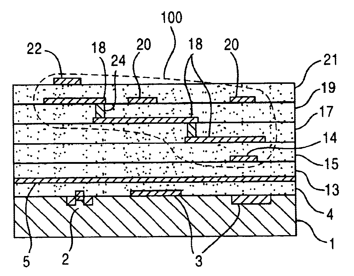
FIG. 3A shows a plan view of an MMIC according to an embodiment of the present invention, and FIG. 3B shows a cross-sectional view taken along the line IIIB—IIIB in FIG. 3A. The MMIC has an active device 2 such as an HEMT and passive devices 3 such as a metal-insulator-metal (MIM) capacitor and a resistor which are formed on a GaAs substrate 1. A surface insulating layer 4 for protection from the external atmosphere is formed on the devices 2 and 3. A stable material such as silicon nitride is used as the surface insulating layer 4. A ground plate 5 having a potential fixed to the ground potential is formed on the surface insulating layer 4. A first level insulating interlayer 6, a first level wiring layer 7, a second level insulating interlayer 8, a separation electrode 9, a third level insulating interlayer 10, and a second level wiring layer 11 are formed above the ground plate 5....


PUM


Abstract

A high frequency semiconductor device including wiring layers which are formed above a semiconductor substrate and in which transmission lines are formed by combining with a ground plate having a potential fixed at the ground potential, at least one crossing portion in which the wiring layers mutually cross, with insulating interlayers provided therebetween, and at least one separation electrode being selectively provided on one of the insulating interlayers, the at least one separation electrode having a potential fixed at the ground potential. Accordingly, in the high frequency semiconductor device, electrical interference between two crossing wiring layer is prevented and transmission loss is suppressed.

Description

BACKGROUND OF THE INVENTION1. Field of the InventionThe present invention relates to high frequency semiconductor devices, and in particular, to a multilayer wiring structure for monolithic microwave integrated circuit (MMIC) for use in the gigahertz or higher frequency spectrum.2. Description of the Related ArtIn an MMIC in which high speed semiconductors such as high-electron-mobility transistors (HEMTs) and hetero-bipolar transistors (HBTs) are integrated with passive devices such as capacitors and resistors, microstrip transmission lines which have superior signal transmission characteristics in high frequency region are generally used for transmitting signals among devices. For increasing the integration density of the MMIC, the transmission lines are normally multilayered.FIGS. 1A and 1B show the structure of an MMIC according to the related art. FIG. 1A shows a plan view of the MMIC, and FIG. 1B shows a cross-sectional view taken along the line IB—IB in FIG. 1A. As shown in F...

Claims


Application Information

Patent Timeline
IPC IPC(8): H01L23/522H01L23/58H01L23/552H01L23/52H01L23/66H01L21/768H01L21/82H01L21/822H01L27/04H01P3/08
CPCH01L23/5222H01L23/5225H01L23/552H01L23/66H01L2924/0002H01L2924/3011H01L2924/00
Inventor BABA, OSAMUMIMINO, YUTAKA
Owner FUJITSU QUANTUM DEVICES LTD
Why Eureka
Try Eureka