Method and amplification circuit with pre-emphasis

a technology of amplification circuit and pre-emphasis, applied in the direction of amplification control details, transmission, electric pulse generator, etc., can solve the problems of difficult outputting of signals of extremely high frequency, more problems, and critical handling of off-chip electrical signals, so as to improve the performance of circuits

Inactive Publication Date: 2005-02-08
STMICROELECTRONICS SRL
View PDF5 Cites 23 Cited by
  • Summary
  • Abstract
  • Description
  • Claims
  • Application Information

AI Technical Summary

Benefits of technology

In view of the foregoing background, an object of the present invention is to provide a method and corresponding amplification circuit for amplifying with pre-emphasis to overcome the above mentioned synchronization problems, and to improve the performance of circuits implementing pre-emphasis techniques.
A main feature of the present invention is to increase the gain at each switching edge of the signal to be transmitted by using a driver with pre-emphasis that combines the signal to be transmitted with a delayed replica thereof. The driver does not have any sub-circuits to be connected and disconnected at each switching of the signal to be transmitted.
More precisely, an object of the present invention is to provide a method for amplifying with pre-emphasis a digital signal representing data to be transmitted through a line driver with pre-emphasis. The gain may vary from a pre-established upper value to a lower value, as well as varying the other way around. The method comprises varying the gain of the line driver with pre-emphasis by setting it at its upper value when coinciding with each switching of the digital signal, and reducing it to its lower value in absence of switching of the digital signal.

Problems solved by technology

As far as the so-called “system on chip” is concerned, the handling of off-chip electrical signals is more critical and poses more problems than the handling of on-chip signals.
This was motivated by the difficulty of outputting signals of extremely high frequency, especially when they are to be conveyed over a long conduction line of a printed circuit board and / or over a long cable having a low matching impedance.
Upon increasing the frequency beyond 1 GHz another problem becomes relevant.
This may cause significant attenuations due to poor dielectrics as the frequency increases.
This technique has the drawback of requiring a good synchronization of the turning on of switches 60 and 62 with the switching edges of the signal to be transmitted.
This is complicated because of the turn-on delays of the switches.
In this second case, the problem is to synchronize the turning on of the second current mirror with the switching edges of the signal to be transmitted.
Consequently, this limits the transmission speed.

Method used


Image

  • Method and amplification circuit with pre-emphasis
  • Method and amplification circuit with pre-emphasis
  • Method and amplification circuit with pre-emphasis

Examples


Embodiment Construction

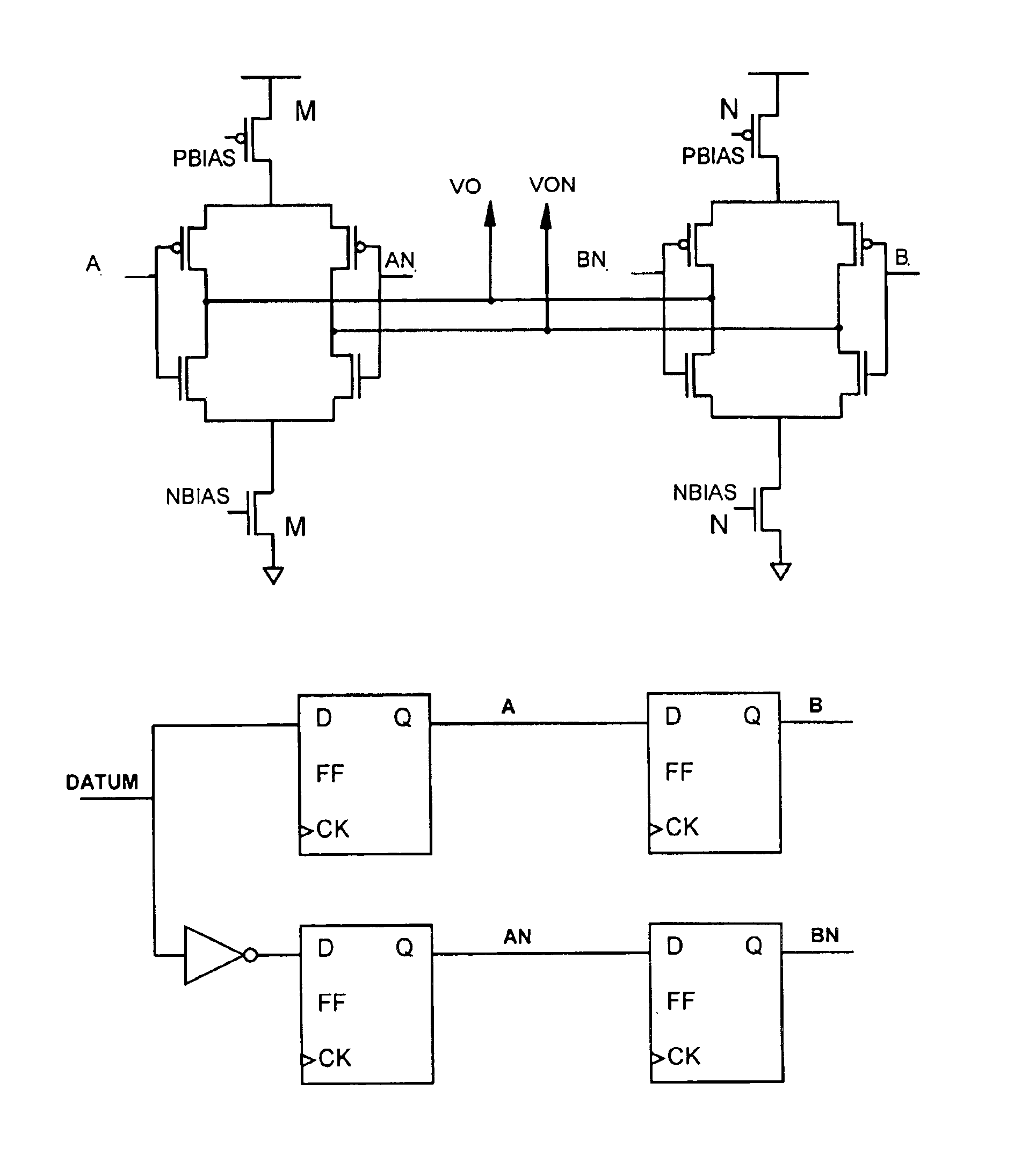
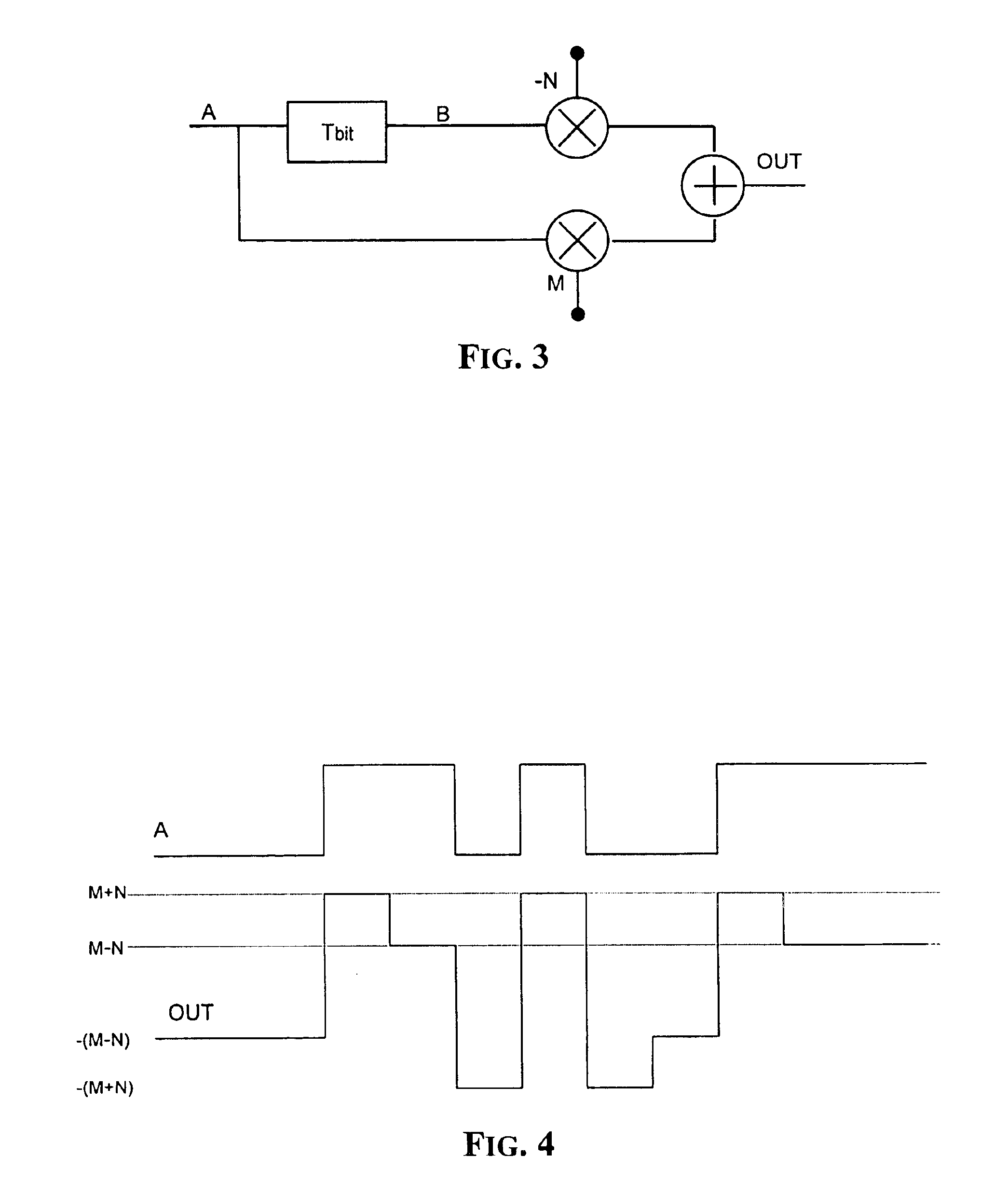
An advantageous feature of the present invention includes generating the amplified digital signal that is transmitted over an output line as the weighted algebraic sum of the input digital signal to be transmitted and a delayed replica thereof. Referring now to FIG. 3, a basic diagram of the amplification circuit with pre-emphasis in accordance with the present invention is shown. The label A indicates the digital signal to be transmitted, and the label OUT is the output signal that may be either a full-swing or a LVDS signal. The output signal OUT is the difference signal between an amplified replica with a certain gain M of the signal A to be transmitted, and an amplified replica with a certain gain N smaller than M, of a delayed replica B of the signal A.

The novel architecture of the present invention does not require sub-circuits to be switched in or out of the functional amplifying circuit at each transition of the signal A. The digital signal A is desirably amplified with an e...


PUM


Abstract

A method for amplifying a digital signal representative of data to be transmitted by a line driver with pre-emphasis over an output line is provided. The gain of the line driver is varied between an upper value to coincide with switching of the digital signal and a lower value in absence of the digital signal switching. In particular, the varying includes amplifying the digital signal with a first gain for generating an amplified digital signal, delaying the digital signal with a predetermined delay for generating a delayed digital signal, and amplifying the delayed digital signal with a second gain for generating a delayed and amplified digital signal. An ouput signal corresponding to a difference between the amplified digital signal and the delayed and amplified digital signal is output over the output line.

Description

FIELD OF THE INVENTIONThe present invention relates in general to output stages of electronic circuits, and in particular, to an amplification circuit with pre-emphasis.BACKGROUND OF THE INVENTIONIn the majority of electronic systems, speed is a fundamental parameter among the parameters that determine the global performance of an electronic system. As far as the so-called “system on chip” is concerned, the handling of off-chip electrical signals is more critical and poses more problems than the handling of on-chip signals.The need of reliably achieving very high communication frequencies has led to the abandonment of CMOS full-swing signals (that is, signals that vary from the negative voltage supply Vss to the positive voltage supply Vdd). This was motivated by the difficulty of outputting signals of extremely high frequency, especially when they are to be conveyed over a long conduction line of a printed circuit board and / or over a long cable having a low matching impedance.The s...

Claims


Application Information

Patent Timeline
Patent Type & Authority Patents(United States)
IPC IPC(8): H03G1/00H03K5/24H04L25/02
CPCH03G1/0029H04L25/0286H03K5/2481H04L25/0272
Inventor DE LAURENTIIS, PIERPAOLOTOMASINI, LUCIANOCATTANEO, CLAUDIO
Owner STMICROELECTRONICS SRL
Why Eureka
Try Eureka