Polishing method and polishing apparatus

Inactive Publication Date: 2005-02-15
SONY CORP
View PDF3 Cites 2 Cited by
  • Summary
  • Abstract
  • Description
  • Claims
  • Application Information

AI Technical Summary

Benefits of technology

An object of the present invention is to provide a polishing method and a polishing apparatus capable of easily flattening unevenness formed on the surface of a film and able to efficiently polish the film flat while suppressing damage to an interlayer insulating film below a copper film when flattening the copper film or other film by polishing to form copper interconnections etc. in a semiconductor device.
Here, when all of the copper film on the barrier metal film at the outside of the interconnection grooves is removed and the barrier metal film is exposed, since the resistance of the barrier metal film is usually larger than that of copper, the current value starts to fall from its maximum level after the removal of the chelate film, so by stopping the application of voltage when it starts to fall, it is possible to stop the formation of the chelate film by subsequent anodic oxidation and therefore possible to manage the progress of polishing.

Problems solved by technology

Further, the amount of the processing solution in contact and acting there itself is small.

Method used


Image

  • Polishing method and polishing apparatus
  • Polishing method and polishing apparatus
  • Polishing method and polishing apparatus

Examples


first embodiment

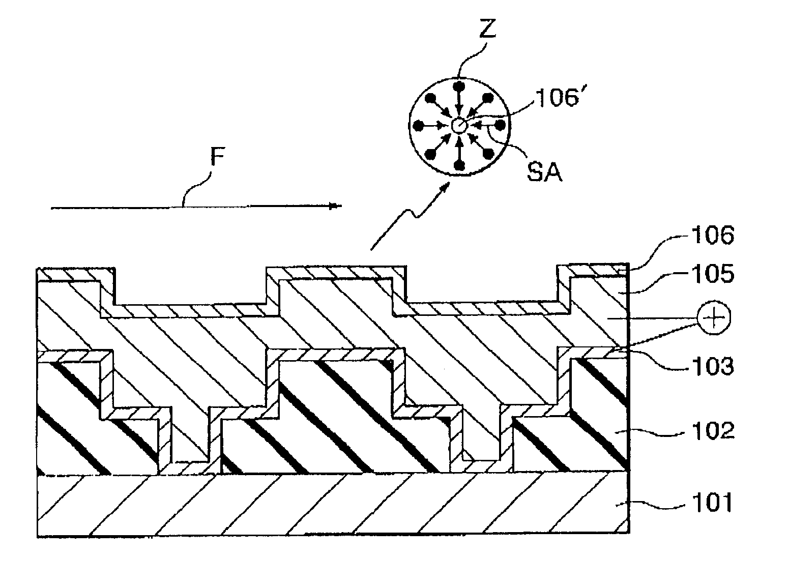
The first embodiment relates to application of the polishing method of the present invention to a process of formation of copper interconnections by a dual damascene process in a process of production of a semiconductor device.

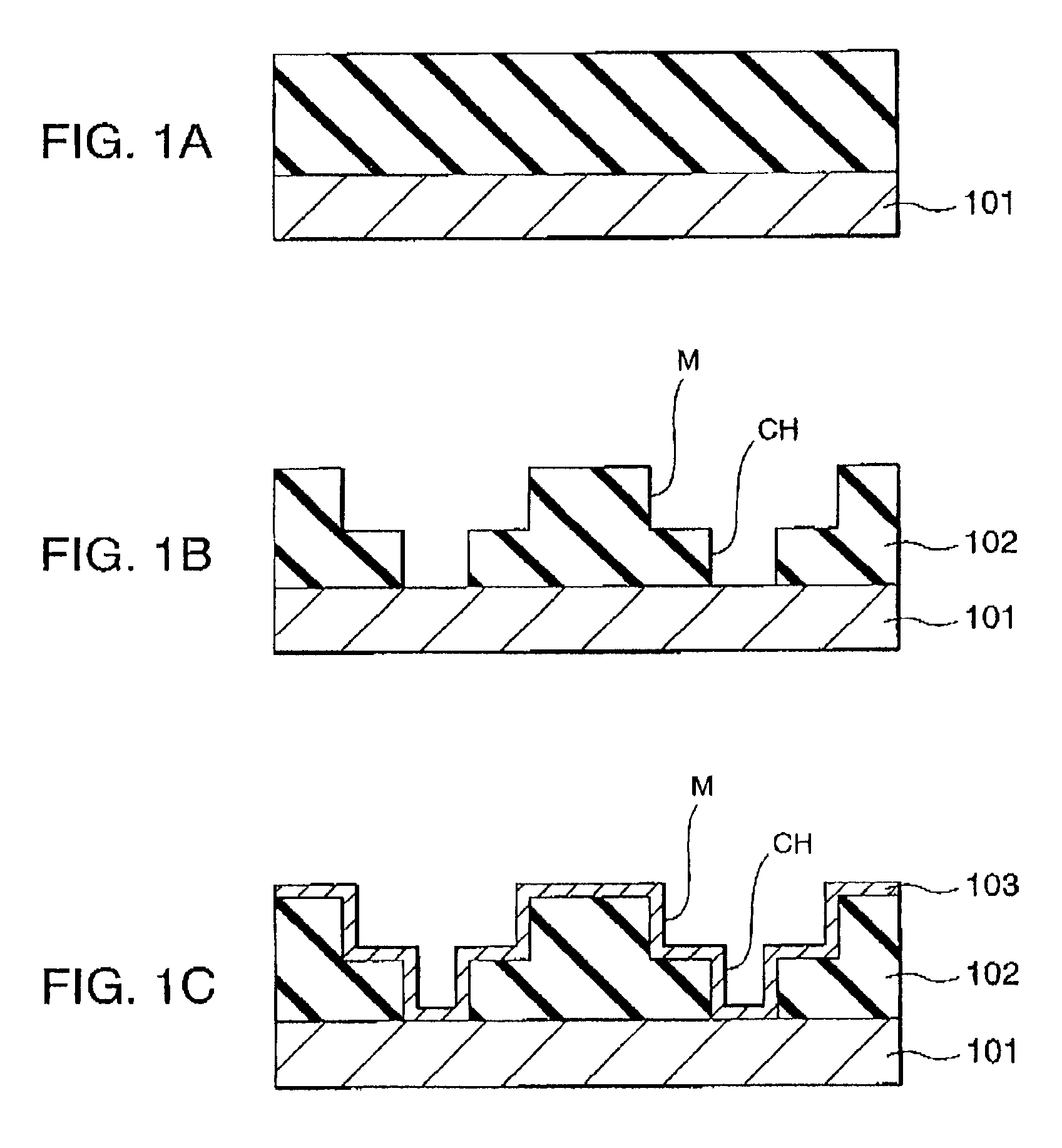
First, as shown in FIG. 1A, for example an interlayer insulating film 102 made of for example silicon oxide is formed by low pressure chemical vapor deposition (CVD) on a silicon or other semiconductor substrate 101 on which a not illustrated impurity diffusion region is suitably formed by using for example tetraethyl orthosilicate (TEOS) as a reaction source.

Next, as shown in FIG. 1B, contact holes CH communicating with the impurity diffusion region of the semiconductor substrate 101 and interconnection grooves M are formed by well-known photolithography and etching. The depth of the interconnection use grooves M is for example about 800 nm.

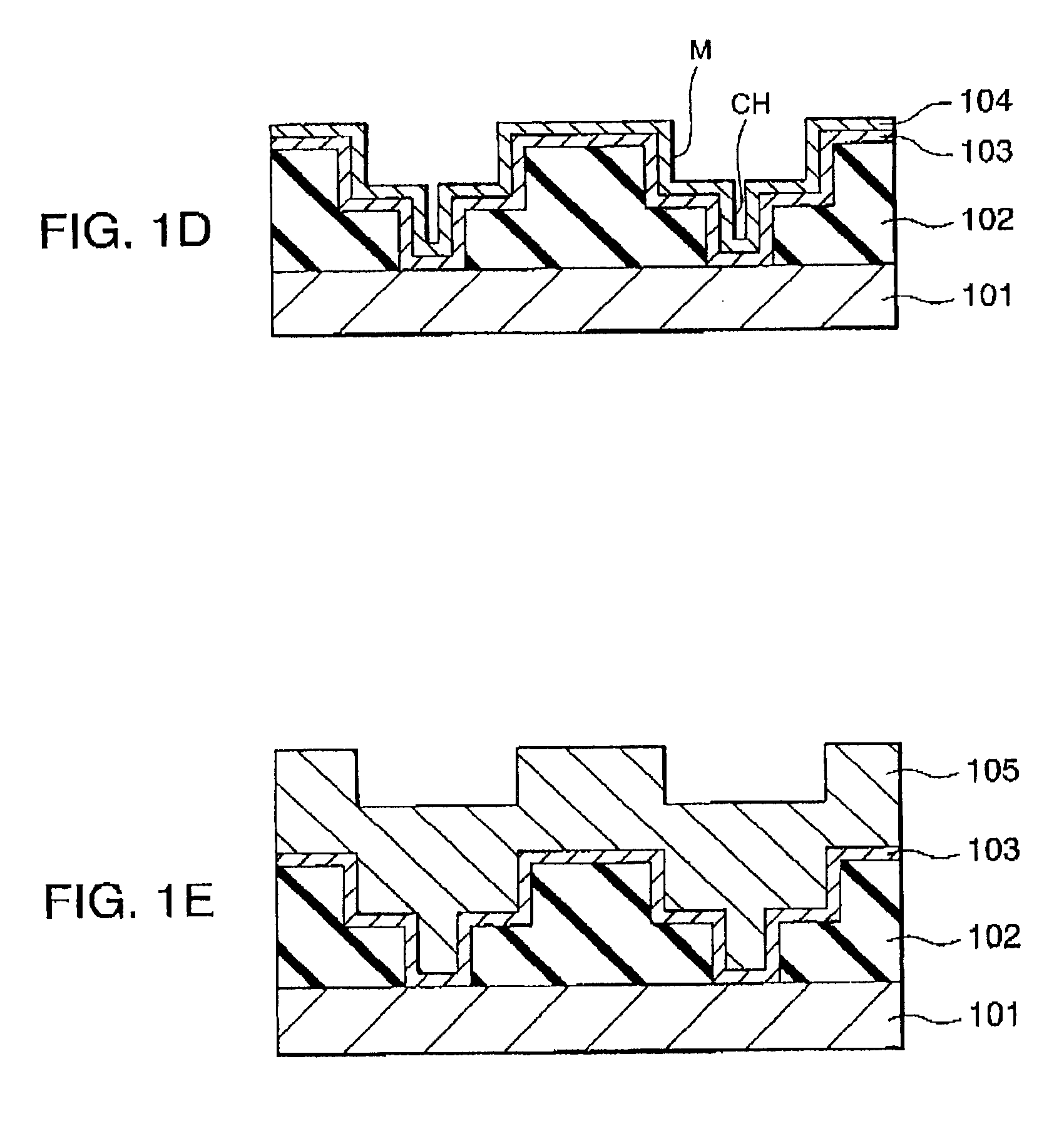
Next, as shown in FIG. 1C, a barrier metal film 103 is formed on the surface of the interlayer insulating film 102 and i...

second embodiment

FIG. 3 is a schematic view of the configuration of a polishing apparatus used in the process of polishing a copper film of the above interconnection layer.

Namely, the polishing apparatus of the present embodiment includes a table 10 for carrying a wafer W to be polished (hereinafter, also referred to as “wafer”) that has a copper film on its surface, a securing means such as a vacuum chuck provided on the table 10, a controller 23, a control panel 24, a power supply 25, an ammeter 26, a cathode member E, an electrolytic bath tank T for storing the electrolytic solution EL, a jet pump P, a filter FT, and an electrolytic solution pipe PEL.

Note that, although not illustrated in the figure, the above polishing apparatus is installed in a clean room, and a loading / unloading port for loading and unloading a wafer cassette storing wafers to be polished in or out of the clean room is provided in the clean room. Further, a wafer conveyance robot for transferring the wafers between the wafer ...

third embodiment

FIG. 6 is a schematic view of the configuration of a polishing apparatus according to a third embodiment.

The polishing apparatus according to this embodiment is similar to the polishing apparatus according to the second embodiment, but the cathode member E is formed as a hollow cylindrical nozzle N. Electrolytic solution EL is jetted from a slit SL provided in the nozzle N.

With the above configuration, the wafer and the cathode member E do not necessarily have to be immersed in the electrolytic solution EL stored in the tank. It is sufficient that the electrolytic solution EL supplied from the slit SL of the nozzle N contact both of the wafer W and the cathode member E to enable current to be conducted between the two.

The rest of the configuration is substantially the same as that of the polishing apparatus of the second embodiment.

FIG. 7A is a sectional view in a plane vertical to the longitudinal direction of the hollow cylindrical nozzle N functioning as the cathode member, FIG. ...


PUM

PropertyMeasurementUnit
Shear stressaaaaaaaaaa

Abstract

A polishing method able to easily flatten unevenness formed on the surface of a film to be polished and able to efficiently polish the film flat while suppressing damage to an interlayer insulating film below the film, comprising, when polishing an object having a film such as an interconnection layer formed burying interconnection grooves formed in an insulating film of a substrate, supplying a polishing solution over the surface to be polished at least substantially parallel to the surface to preferentially remove by polishing the projecting portions of the film and flatten the surface by the shear stress of the processing solution or arranging a cathode member facing the surface and supplying an electrolytic solution containing a chelating agent between the surface and cathode member while supplying voltage between the film and the cathode member to preferentially remove by polishing the projecting portions of the film and flatten the surface by the shear stress of the electrolytic solution, and a polishing apparatus using the same.

Description

RELATED APPLICATION DATAThe present application claims priority to Japanese Application(s) No(s). P2000-294974 filed Sep. 27, 2000, which application(s) is / are incorporated herein by reference to the extent permitted by law.BACKGROUND OF THE INVENTION1. Field of the InventionThe present invention relates to a polishing method and polishing apparatus, a more particularly relates to a polishing method and polishing apparatus for flattening an uneven surface formed along with formation of copper interconnections in the process of production of a semiconductor device having copper interconnections.2. Description of the Related ArtAlong with the increase in integration and reduction of size of semiconductor devices, progress has been made in miniaturization of interconnections, reduction of interconnection pitch, and superposition of interconnections. The importance of the multilayer interconnection technology in the manufacturing process of semiconductor devices is therefore rising.To f...

Claims


Application Information

Patent Timeline
IPC IPC(8): B24B37/04H01L21/02H01L21/321H01L21/70H01L21/768H01L21/304B23H5/08
CPCB24B37/042H01L21/3212H01L21/76807
Inventor SATO, SHUZOSEGAWA, YUJIYOSHIO, AKIRANOGAMI, TAKESHI
Owner SONY CORP
Why Eureka
Try Eureka