Glass substrate and leveling thereof

Inactive Publication Date: 2005-02-15
SHIN ETSU CHEM IND CO LTD
View PDF9 Cites 23 Cited by
  • Summary
  • Abstract
  • Description
  • Claims
  • Application Information

AI Technical Summary

Benefits of technology

An object of the invention is to provide a glass substrate having an improved surface flatness and a glass

Problems solved by technology

This leads to a failure to establish fine-circuitry devices.
This is because in the traditional polishing technology, it is possible to roughly control the polishing rate over the entire surface of a substrate, but it is impossible in a practical sense to specify a leveling recipe for each of starting substrates in accordance with their shape and individually polish the substrates for evening out irregularitie

Method used


Image

  • Glass substrate and leveling thereof
  • Glass substrate and leveling thereof
  • Glass substrate and leveling thereof

Examples


example 1

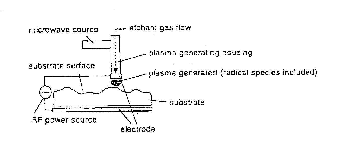
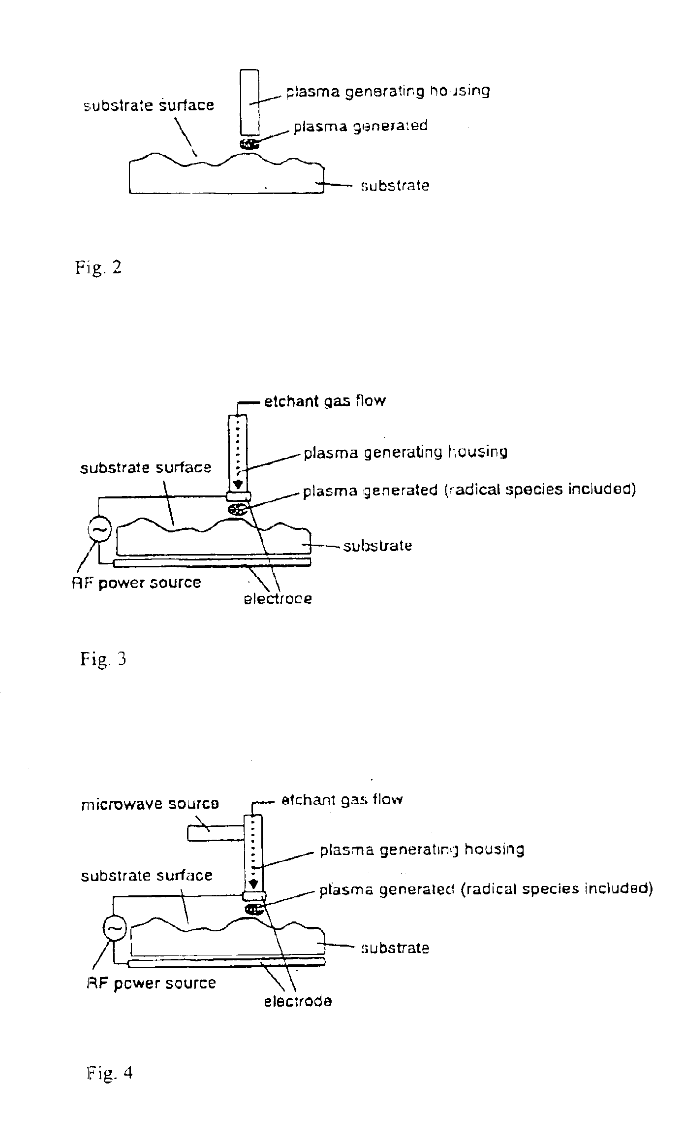
The starting substrate used was a quartz substrate having a pair of square surfaces of 152 mm by 152 mm and a thickness of 6.35 mm.

One surface of the quartz substrate was measured by an optical interference flatness meter, finding a flatness of 3.7 nm / cm2 of the surface. Based on the thus obtained data about microscopic peaks and valleys on the substrate surface, the rate of movement of a plasma generating housing which was located above the substrate was computed. Plasma etching was carried out on the substrate surface by moving the plasma generating housing along the substrate surface at the controlled rate. The plasma generating housing of high-frequency type (150 W) had cylindrical electrodes of 75 mm diameter. The etchant gas used was methane tetrafluoride. After plasma etching was carried out over the entire substrate surface, that surface of the quartz substrate was measured again by the optical interference flatness meter, finding a flatness of 0.21 nm / cm2 of the surface.

examples 2-9

As in Example 1, quartz substrates having surfaces with different flatness values were plasma etched, obtaining quartz substrate having surfaces leveled. The flatness values per square centimeter of the surface before and after plasma etching are shown in Table 1.

TABLE 1 Example23456789Initial flatness5.24.02.33.23.34.12.91.5(nm)Flatness after0.740.480.170.390.520.820.390.04plasma etching(nm)

The invention ensures that quartz substrates having a surface leveled to a flatness of 0.04-1.3 nm / cm2 of the surface are readily produced.


PUM

PropertyMeasurementUnit
Heightaaaaaaaaaa
Plasma poweraaaaaaaaaa

Abstract

A glass substrate having a surface which has been leveled, preferably to a flatness of 0.04-1.3 nm/cm2 of the surface, by local plasma etching is provided. A glass substrate whose surface carries microscopic peaks and valleys is leveled by measuring the height of peaks and valleys on the substrate surface, and plasma etching the substrate surface while controlling the amount of plasma etching in accordance with the height of peaks.

Description

This invention relates to glass substrates which are useful as silica glass substrates for reticles used in the most advanced application among semiconductor-related electronic materials, and silica glass substrates or silica glass chips which are expected to find wide-spreading use in the fields of microelectronics, micro-optics and microanalyses; and a method for leveling the surface thereof.BACKGROUND OF THE INVENTIONQuality parameters of photomask-forming silica glass substrates include the size of defects, the density of defects, flatness, surface roughness, the opto-chemical stability of material, and the chemical stability of surface. Of these parameters, the quality relating to the flatness on substrates is more strictly required to comply with the trend of ICs toward finer-circuitry. It is highly probable that the design rule of interconnection to be transferred to silicon wafers will fall below 100 nm. Then, silica glass substrates for photomasks must have a flatness below...

Claims


Application Information

Patent Timeline
IPC IPC(8): C03C15/00C03C23/00C03C19/00G03F1/60H01L21/027
CPCC03C15/00C03C23/006C03C19/00C03C2204/08
Inventor TAKEUCHI, MASAKISHIBANO, YUKIO
Owner SHIN ETSU CHEM IND CO LTD
Why Eureka
Try Eureka