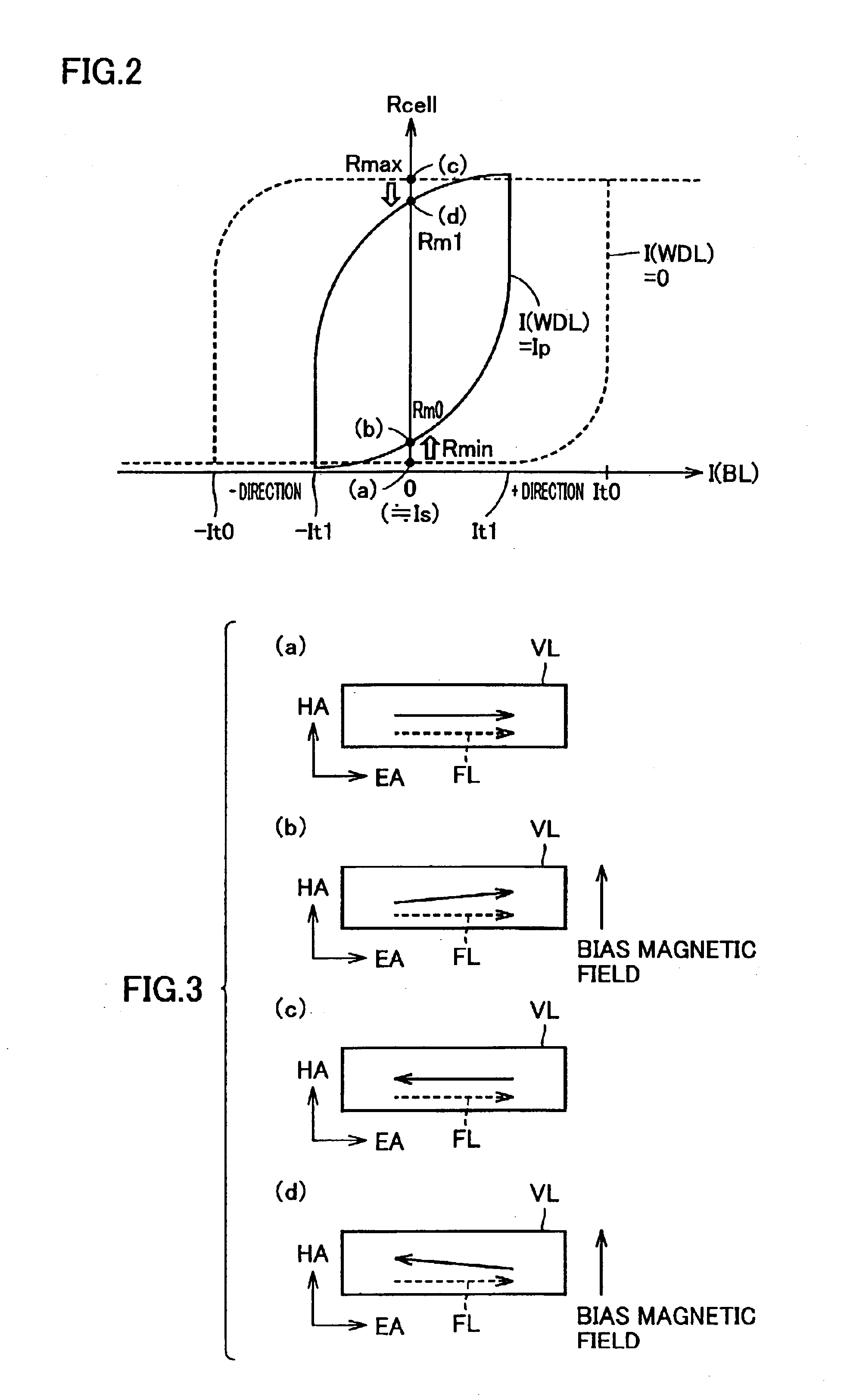
[0035]Therefore, a main
advantage of the present invention is as follows: when a bias
magnetic field along the hard axis direction is applied to a selected memory cell, the electric resistance of the selected memory cell changes in the positive or negative direction (rises or falls) depending on the storage
data level. By using such a property, self-reference read operation can be conducted at a high speed by merely accessing the selected memory cell. In other word, forcible write and read operations and rewrite operation of the storage data to the selected memory cell are not required.
[0036]Moreover, a precharge
voltage of the data line (first prescribed
voltage) and a precharge voltage of the first and second sense input nodes in the balanced state before application of the bias magnetic field (second prescribed voltage) can be independently set to optimal values. Accordingly, the precharge voltage of the data line is set to an optimal level in view of MR (
Magneto-Resistive) characteristics in the memory cell, whereas the precharge voltage of the first and second sense amplifiers can be set to such a level that assures an operation margin of the sense
amplifier.
[0037]According to another aspect of the present invention, a thin film
magnetic memory device includes a plurality of memory cells, a data line, a current supply circuit, a bias magnetic field applying section, and a data read circuit. Each of the plurality of memory cells is magnetized along an easy axis in a direction corresponding to storage data magnetically written therein, and has an electric resistance corresponding to a
magnetization direction. The data line is electrically coupled to a fixed voltage through a selected one of the plurality of memory cells in read operation. The current supply circuit couples the data line to a prescribed voltage at least in the read operation. The bias magnetic field applying section applies a bias magnetic field along a hard axis to the selected memory cell in the read operation, and applies a data write magnetic field along the hard axis to a selected memory cell in the write operation. The bias magnetic field applying section includes a plurality of current lines, a plurality of driver transistors, and a plurality of current line drive control sections. The plurality of current lines are each provided for every prescribed block of the plurality of memory cells, and each selectively receives a current for applying a magnetic field of a direction along the hard axis to each of corresponding memory cells. The plurality of driver transistors are provided corresponding to the plurality of current lines and each is connected in series with corresponding one of the plurality of current lines between first and second voltages. Each of the current line drive control sections controls ON / OFF of corresponding one of the driver transistors. The plurality of current line drive control sections are provided corresponding to the plurality of current lines and each includes a
control circuit for controlling a driver current of corresponding one of the plurality of driver transistors according to address information indicating whether the corresponding current line corresponds to the selected memory cell or not. The
control circuit causes the driver current to change more slowly in the read operation than in the write operation. The data read circuit produces read data corresponding to storage data of the selected memory cell, based on voltages on the data line before and after application of the bias magnetic field to the selected memory cell in the read operation.
[0038]When a bias magnetic field along the hard axis direction is applied to a selected memory cell, the electric resistance of the selected memory cell changes in the positive or negative direction (rises or falls) depending on the storage
data level. By using such a property, the above thin film
magnetic memory device can conduct self-reference read operation at a high speed by merely accessing the selected memory cell. In other word, forcible write and read operations and rewrite operation of the storage data to the selected memory cell are not required. Moreover, since the structure for generating a bias magnetic field can also be used to generate a prescribed data write magnetic field in write operation, the circuit structure can be simplified. Especially, since a bias magnetic field is gradually generated in read operation, abrupt change in data line voltage is prevented, whereby stable read operation with reduced noises can be implemented.
[0039]According to still another aspect of the present invention, a thin film magnetic memory device includes a plurality of memory cells, a data line, a current supply circuit, a magnetic field applying section, and a data read circuit. Each of the plurality of memory cells is magnetized along an easy axis in a direction corresponding to storage data magnetically written therein, and has an electric resistance corresponding to a
magnetization direction. The data line is electrically coupled to a fixed voltage through a selected one of the plurality of memory cells in read operation. The current supply circuit couples the data line to a prescribed voltage at least in the read operation. The magnetic field applying section receives a first
power supply voltage and applies a predetermined magnetic field along a hard axis to the selected memory cell in each of write operation and read operation. The data read circuit receives a second
power supply voltage and the fixed voltage, and produces read data corresponding to storage data of the selected memory cell. A difference between the first
power supply voltage and the fixed voltage is larger than a difference between the second power supply voltage and the fixed voltage.
[0040]When a bias magnetic field along the hard axis direction is applied to a selected memory cell, the electric resistance of the selected memory cell changes in the positive or negative direction (rises or falls) depending on the storage data level. By using such a property, the above thin film magnetic memory device can conduct self-reference read operation at a high speed by merely accessing the selected memory cell. In other word, forcible write and read operations and rewrite operation of the storage data to the selected memory cell are not required. Moreover, since the structure for generating a bias magnetic field can also be used to generate a prescribed data write magnetic field in write operation, the circuit structure can be simplified. Especially, since a current line can be driven with a sufficient voltage difference, a sufficient amount of current can be supplied to generate a bias magnetic field and a data write magnetic field.
