
Enhanced light absorption of solar cells and photodetectors by diffraction

a technology of solar cells and light absorption, applied in the field of solar cells and photodetectors, can solve the problems of limited application of low-cost, multi-crystalline (mc) si, and the inability to benefit from recent advances in diffractive optics, and achieve the effects of increasing improving the performance of thin-film solar cells, and improving the absorption of light radiation

Inactive Publication Date: 2005-02-22
SANDIA NAT LAB
View PDF6 Cites 37 Cited by
  • Summary
  • Abstract
  • Description
  • Claims
  • Application Information

AI Technical Summary

Benefits of technology

[0012]Benefits and advantages of the present method include improved performance of thin-film solar cells, space solar cells, and wavelength-selective photodetectors, where enhanced IR response is required as a result of either insufficient film thickness for light absorption or radiation-induced bulk damage leading to a material having a low lifetime.

Problems solved by technology

Solar cells and photodetectors have not benefited from recent advances in diffractive optics.
Applicability of these texturing processes to thin-films (≦20 μm), and low-cost, multi-crystalline (mc) Si are limited due to their large dimensions and preferential (100) crystal etching mechanisms.
Heine and Morf teaches away from the use of a front surface grating because of surface passivation issues.

Method used


Image

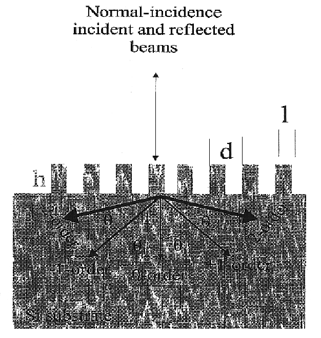
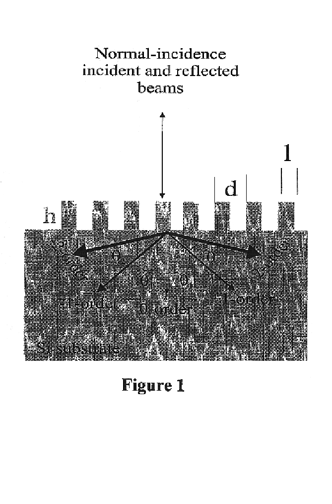
  • Enhanced light absorption of solar cells and photodetectors by diffraction
  • Enhanced light absorption of solar cells and photodetectors by diffraction
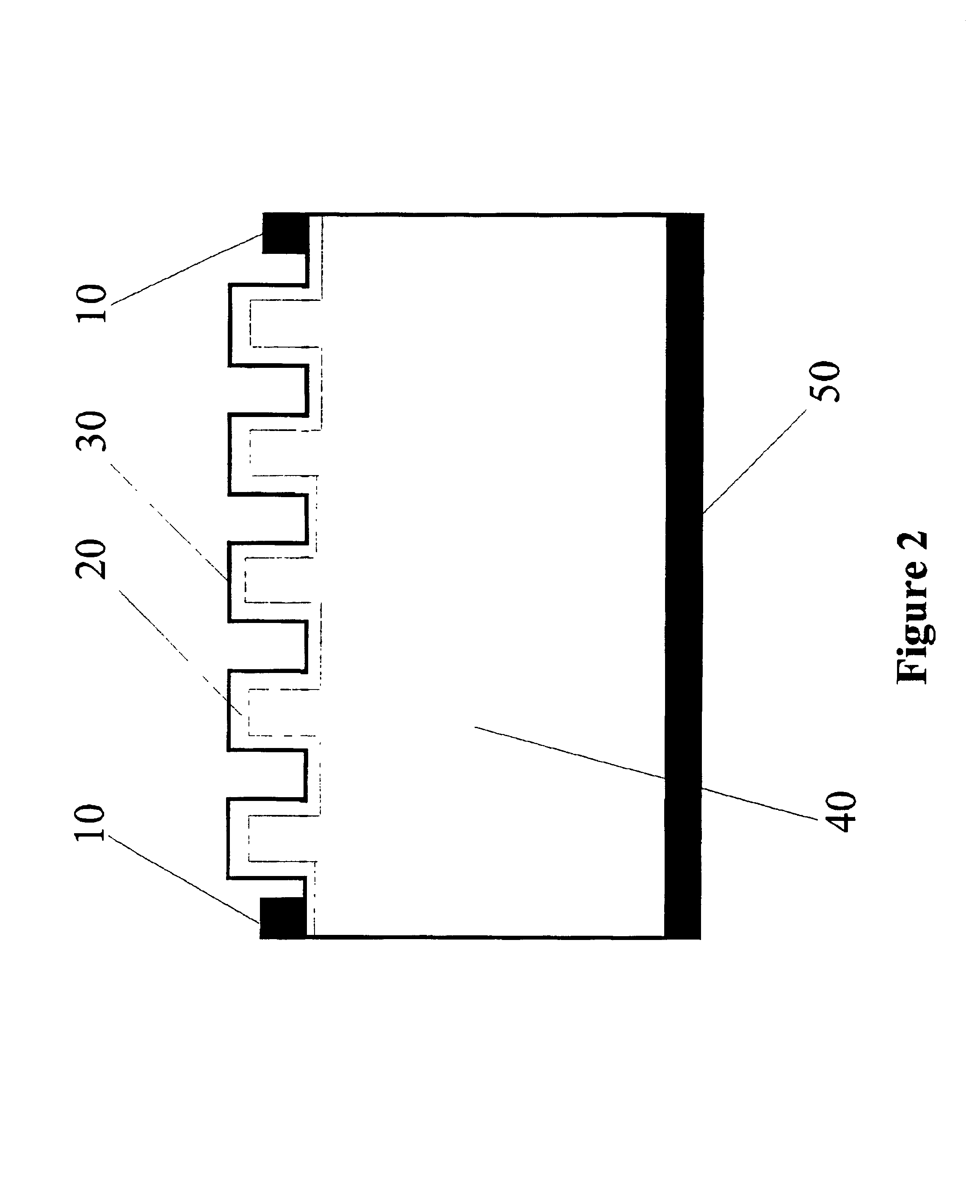
  • Enhanced light absorption of solar cells and photodetectors by diffraction

Examples


Embodiment Construction

t measurements from one-dimensional gratings shown in FIG. 13.

[0028]FIG. 15 shows SEM picture of a random silicon surface formed by maskless reactive ion etching.

[0029]FIG. 16 shows IQE measurements from random RIE surface solar cell, also plotted for comparison is planar surface response.

[0030]FIG. 17 shows IQE measurements from random RIE surface solar cell with ion-implanted surface junction, also plotted for comparison is planar surface response.

[0031]FIG. 18 shows IQE measurements from the same one-dimensional grating solar cells before and after application of anti-reflection films.

[0032]FIG. 19 shows the variation of propagation angles of the transmitted diffraction orders inside silicon, at a fixed period, as a function of wavelength.

[0033]FIG. 20 shows the calculated, polarization-dependent, diffraction efficiencies for 0.65-μm period one-dimensional gratings for rectangular (a) and triangular (b) profiles.

[0034]FIG. 21 shows the calculated, polarization-dependent, diffract...


PUM


Abstract

Enhanced light absorption of solar cells and photodetectors by diffraction is described. Triangular, rectangular, and blazed subwavelength periodic structures are shown to improve performance of solar cells. Surface reflection can be tailored for either broadband, or narrow-band spectral absorption. Enhanced absorption is achieved by efficient optical coupling into obliquely propagating transmitted diffraction orders. Subwavelength one-dimensional structures are designed for polarization-dependent, wavelength-selective absorption in solar cells and photodetectors, while two-dimensional structures are designed for polarization-independent, wavelength-selective absorption therein. Suitable one and two-dimensional subwavelength periodic structures can also be designed for broadband spectral absorption in solar cells and photodetectors. If reactive ion etching (RIE) processes are used to form the grating, RIE-induced surface damage in subwavelength structures can be repaired by forming junctions using ion implantation methods. RIE-induced surface damage can also be removed by post RIE wet-chemical etching treatments.

Description

RELATED CASES[0002]The present patent application claims the benefit of Provisional Patent Application Serial No. 60 / 195,836 filed on Apr. 11, 2000 for “Method Using Diffraction For Increasing Light Absorption By Silicon”.STATEMENT REGARDING FEDERAL RIGHTS[0003]The United States Government has rights in this invention pursuant to Department of Energy Contract No. DE-AC04-94AL85000 with Sandia Corporation.FIELD OF THE INVENTION[0004]The present invention relates generally to solar cells and photodetectors and, more particularly, to selective enhancement of absorption in either a narrowband or wideband spectral range of interest by efficient optical coupling of incident light into obliquely propagating orders inside the material of construction of the solar cell or photodetector.BACKGROUND OF THE INVENTION[0005]Solar cells and photodetectors have not benefited from recent advances in diffractive optics. Random, wet-chemical texturing techniques to form pyramids in the (100) Silicon (S...

Claims


Application Information

Patent Timeline
IPC IPC(8): H01L31/0236H01L31/0232
CPCH01L31/0232H01L31/02363Y02E10/50H01L31/1804Y02E10/547Y02P70/50
Inventor ZAIDI, SALEEM H.GEE, JAMES M.
Owner SANDIA NAT LAB
Learn More