

MOSFET device with in-situ doped, raised source and drain structures
- Summary
- Abstract
- Description
- Claims
- Application Information
AI Technical Summary
Benefits of technology
Problems solved by technology
Method used
Image

Examples
first embodiment
[0035] Formation of Selective Blanket, Epitaxial Layer
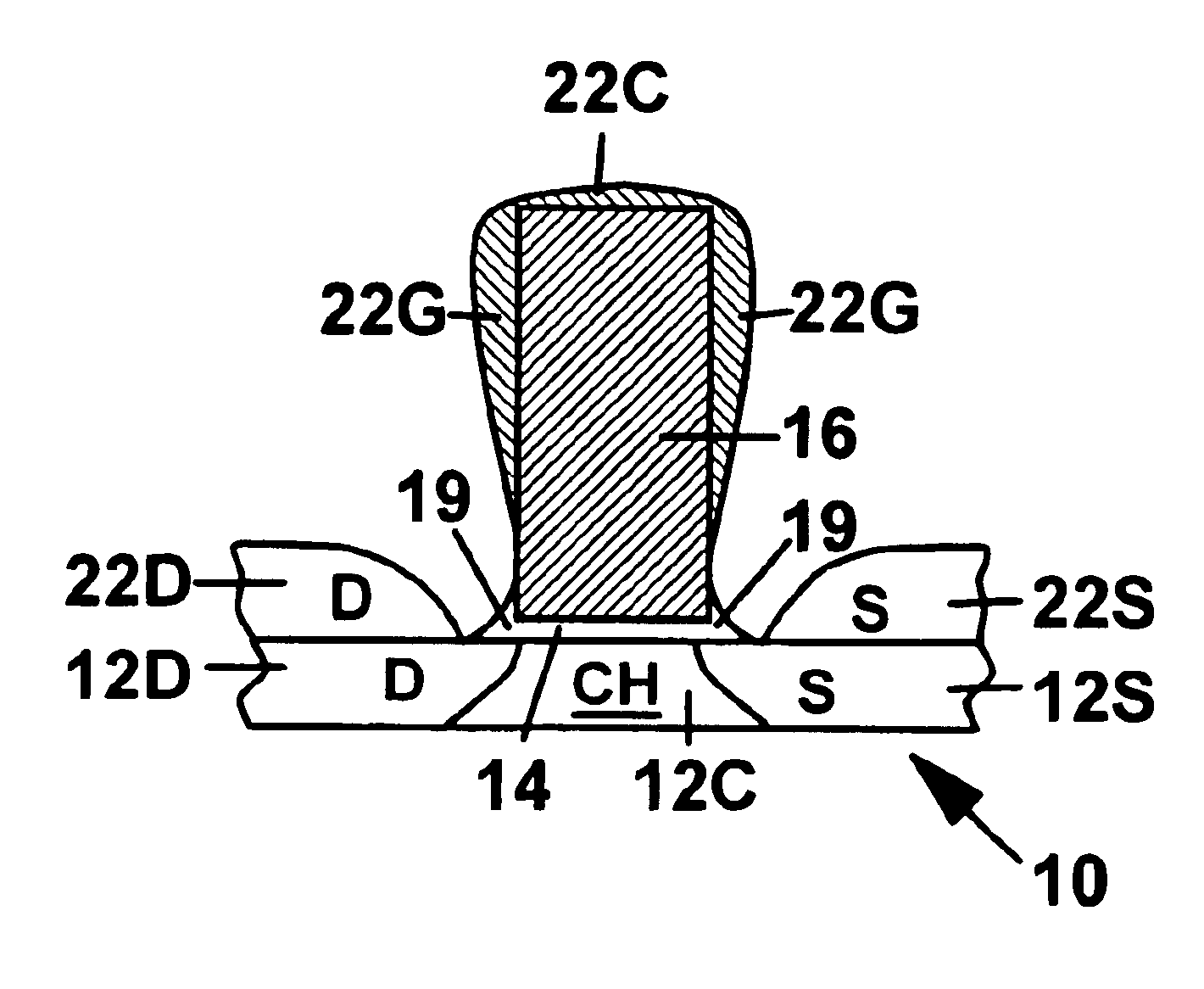
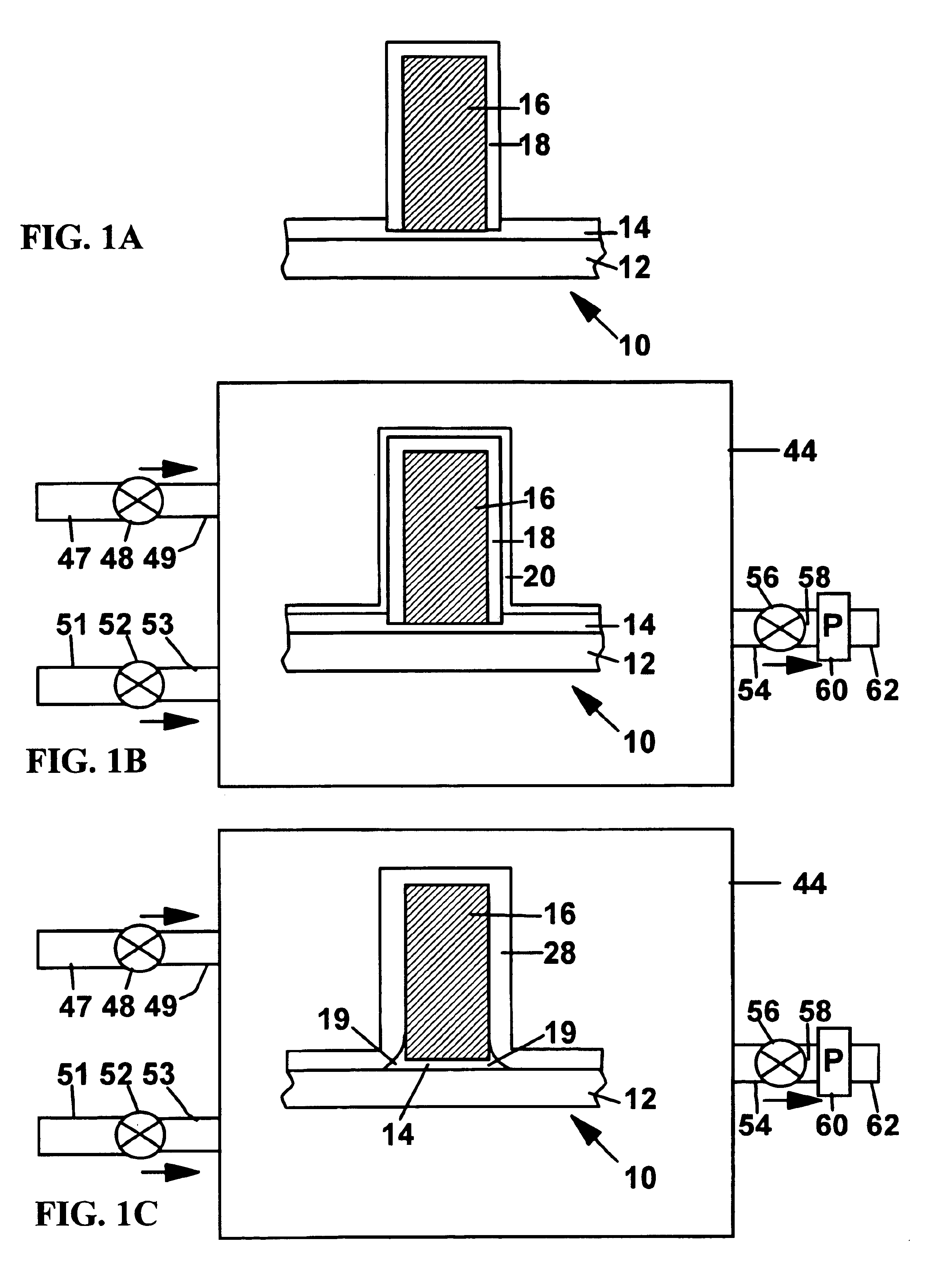
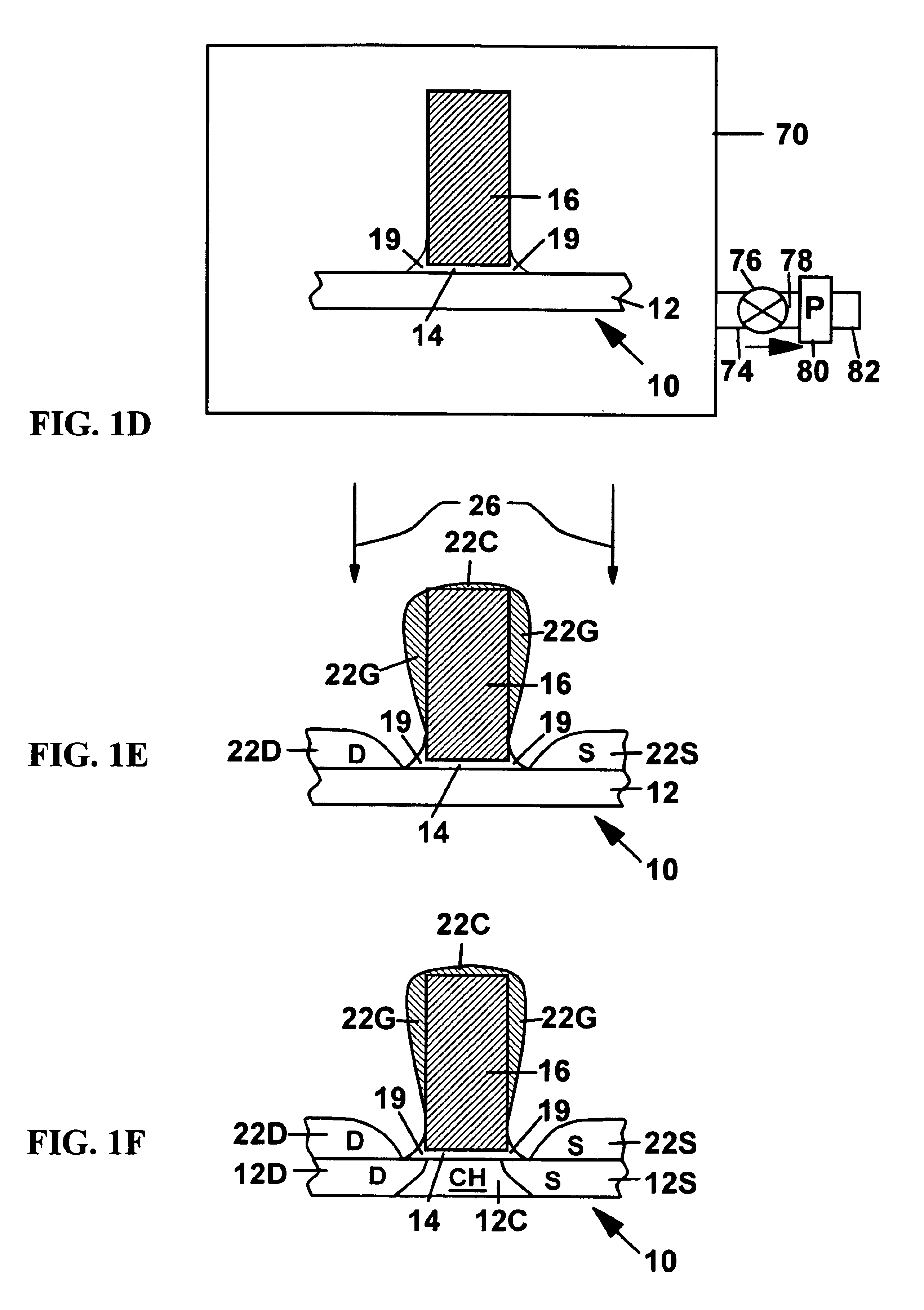
[0036]FIGS. 1A-1F show how an in situ doped, selective epitaxial process can be combined with other processes to form a CMOS device 10 with a set of in situ doped raised source / drain regions 22S / 22D above a set of source / drain regions 12S / 12D formed in the substrate 12.
[0037]FIG. 1A shows the CMOS device 10 in an intermediate stage of processing. The device 10 includes a gate conductor comprising a conventionally doped polysilicon gate electrode 16 formed on a thin film, gate dielectric 14 (e.g. a gate silicon oxide) which is deposited upon the substrate 12, which comprises a single crystal semiconductor in the form of either a bulk layer or a thin film layer of a semiconductor, such as doped silicon. The gate electrode 16 has been patterned by a conventional process such as a polysilicon RIE (Reactive Ion Etching) process employing photolithography as will be well understood by those skilled in the art of MOSFET fabrication proc...
third embodiment
[0072
[0073]FIGS. 3A-3F show an alternative to the process of FIGS. 1A-1F in which a device 10 is made by the process of FIGS. 1A-1F except that the reoxidation step shown in FIG. 1B is omitted when forming the silicon oxide layer 18 over the gate electrode 16 and thickening of the silicon oxide of the gate dielectric layer 14.
[0074]FIG. 3A shows device 10 after formation of the gate electrode 16 over the gate dielectric layer, shown again as a gate oxide layer 14 resting on semiconductor substrate 12 after the process steps described in connection with FIGS. 1A and 1B (other than the reoxidation step). Like reference numbers refer to like elements in FIGS. 1A-1F and other previous drawings and perform similar functions unless otherwise specified. As there was no reoxidation step, surfaces of gate electrode 16 remain exposed and the gate oxide layer 14 is of uniform thickness.
[0075]FIG. 3B illustrates the process of introducing COR gases via lines 49 / 53 into COR chamber 44 to form a ...
PUM
 Abstract
Description
Claims
Application Information