Low-power voltage modulation circuit for pass devices

a low-power voltage and voltage modulation technology, applied in the field of semiconductor devices, can solve the problems of reducing high signal, pmos transistors that are implemented with switches b>40/b>, and pmos transistors that are also affected by disadvantages, so as to achieve easy and optimal compensation, without increasing the power dissipation of semiconductor devices

Inactive Publication Date: 2005-02-22
PANASONIC CORP
View PDF12 Cites 11 Cited by
  • Summary
  • Abstract
  • Description
  • Claims
  • Application Information

AI Technical Summary

Benefits of technology

[0021]Therefore, systems are needed to easily and optimally compensate for the effects of the routing network on the voltages propagated

Problems solved by technology

However, implementing the switches 40 as pass transistors also suffers from a disadvantage.
For example, if a reduced high signal from an NMOS pass transistor is provided to the gate of a PMOS transistor, in an input buffer circuit 80, that has the positive supply voltage Vdd provided on the source, then the reduced high signal will be insufficient to turn the PMOS transistor fully off, and some current will leak through the PMOS transistor.
Similarly, if an increased low signal is provided to the gate of an NMOS transistor, in an input buffer circuit 80, that has the ground voltage Gnd provided on the source, then the increased low signal will be insufficient to turn the NMOS transistor fully off, and some current will leak through the NMOS transistor.
Similar issues arise anytime a high signal is reduced or a low signal is increased as it is propagated across any active or powered device (e.g. transistors, rectifiers, amplifiers, etc.).
Additionally, this extra step typically means that the lower

Method used


Image

  • Low-power voltage modulation circuit for pass devices
  • Low-power voltage modulation circuit for pass devices
  • Low-power voltage modulation circuit for pass devices

Examples


Embodiment Construction

>[0030]FIG. 8 is a depiction of a voltage modulation circuit connected to a CMOS NOR gate, according to an embodiment of the invention.

[0031]FIG. 9 is a depiction of a voltage modulation circuit having a control signal connected to both the converter and the bypass circuit, according to an embodiment of the invention.

[0032]FIG. 10 is a depiction of a voltage modulation circuit which derives the control signal from the inverse of the output of the target circuit, according to an embodiment of the invention.

[0033]FIG. 11 is a graph of the relationship between the length of a transistor and the threshold voltage of the transistor.

[0034]FIG. 12 is a depiction of a reconfigurable device.

DETAILED DESCRIPTION OF THE PREFERRED EMBODIMENTS

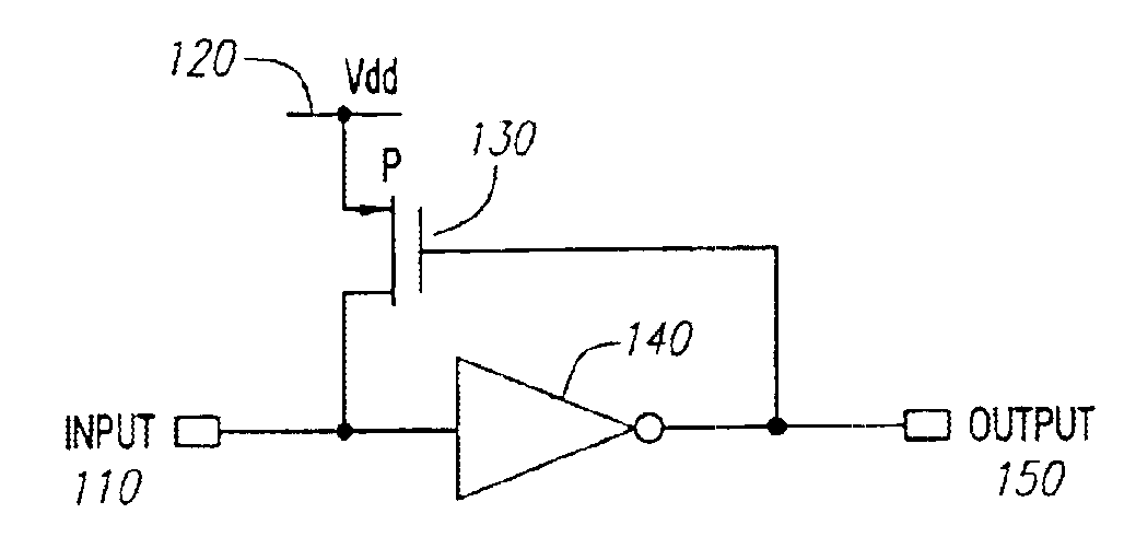
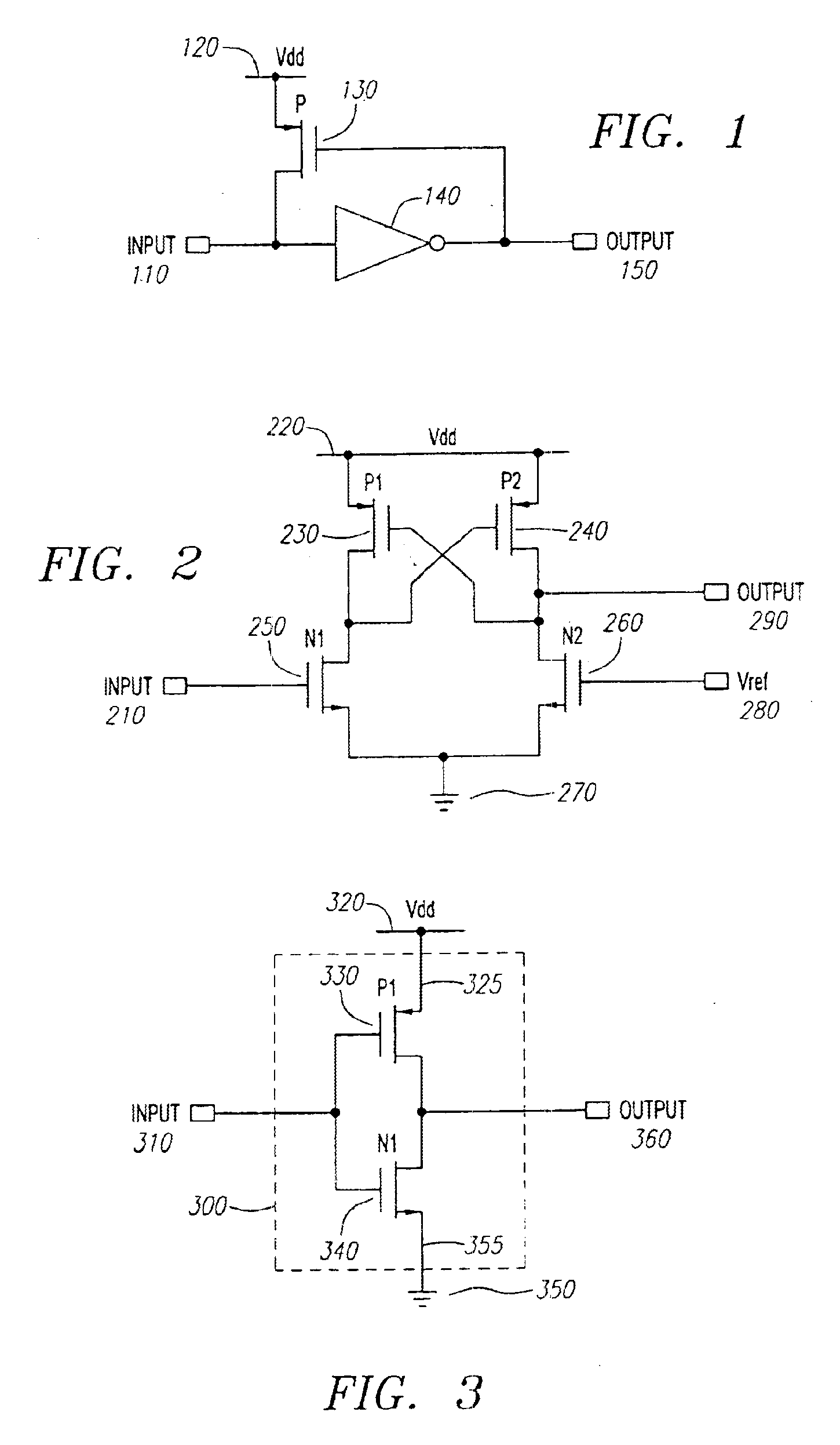
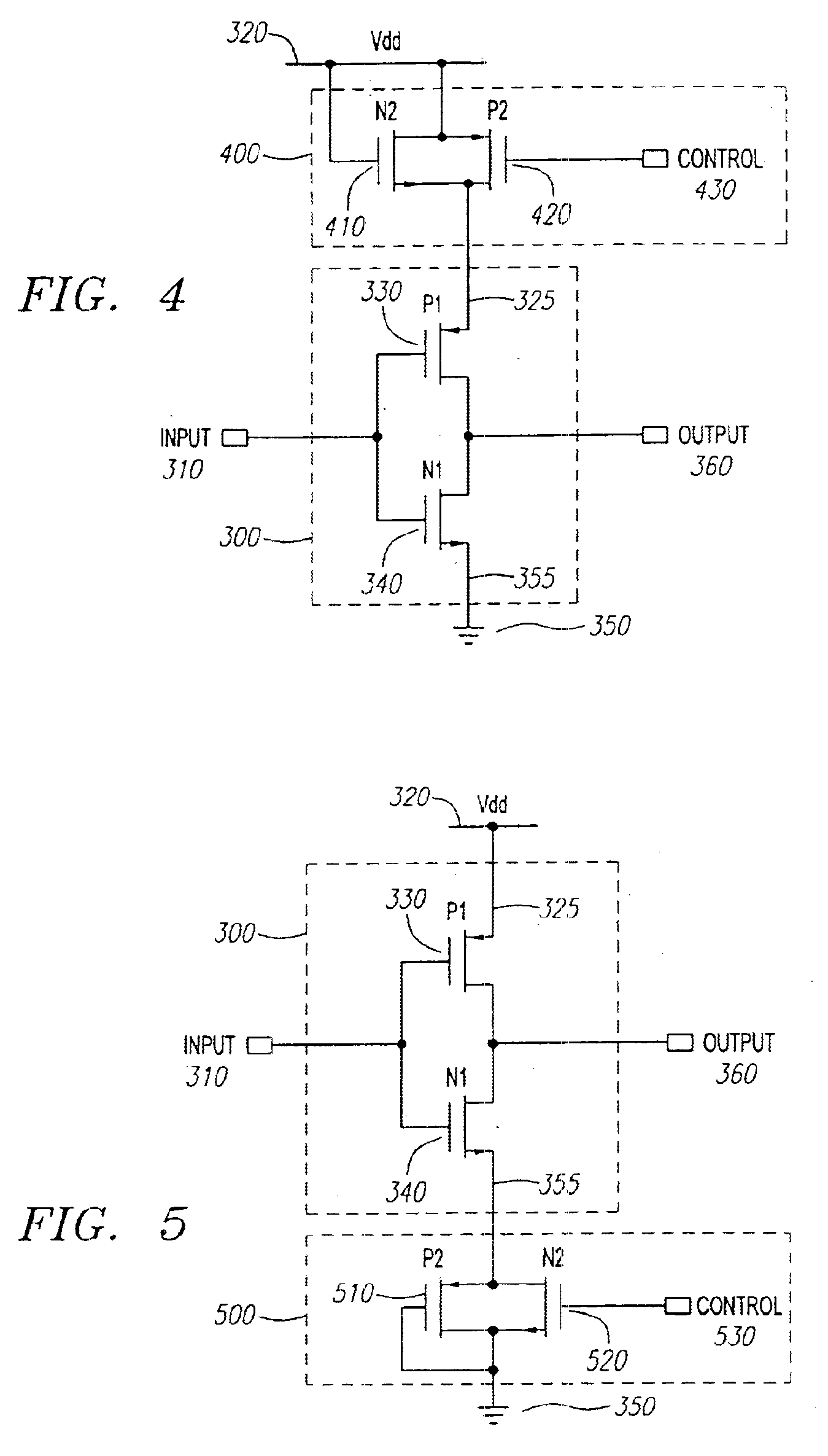
[0035]Turning to FIG. 3, an example CMOS logic device is shown. The logic device of FIG. 3 is an inverter 300, but those skilled in the art will appreciate that the embodiments disclosed herein can be used with any standard logic devices or any combinations...


PUM


Abstract

Power supply voltages are selectively modulated to correspond with degraded input voltages to a logic device. Modulated power supply voltages are provided to transistors within the logic device, so that the degraded input voltages supplied to the transistors are sufficient to turn the transistors substantially on or off. Leakage currents are prevented thereby from flowing across the transistors.

Description

BACKGROUND AND SUMMARY[0002]The invention relates to semiconductor devices. More particularly the invention relates to improvements in the switchable routing networks used in many semiconductor devices to route signals across the device.[0003]Throughout the specification, P and N-channel MOS (metal oxide semiconductor) devices (PMOS and NMOS) are described in terms of their respective gate, drain and source nodes to help clarify the structure and operation of the alternative embodiments. PMOS devices transmit positive current when the signal on the gate is low, and cease transmitting current when the signal on the gate is high. NMOS devices transmit positive current when the signal on the gate is high, and cease transmitting positive current when the signal on the gate is low.[0004]According to standard convention, positive current flows from the drain to the source node in NMOS devices, and flows from the source to the drain in PMOS devices. The source and drain node conventions ar...

Claims


Application Information

Patent Timeline
IPC IPC(8): H03K19/00H03K19/0185H03K19/0948H03K19/173
CPCH03K19/0013H03K19/1733H03K19/018585
Inventor STANSFIELD, ANTHONY I.MARSHALL, ALAN D.
Owner PANASONIC CORP
Why Eureka
Try Eureka