Long wavelength pseudomorphic InGaNPAsSb type-I and type-II active layers for the gaas material system

a material system and active layer technology, applied in the field of vertical cavity surfaceemitting lasers, can solve the problems of poor crystal quality and compressive stain in layers grown on gaas, and achieve the effects of reducing the transition energy, and increasing the efficiency of a quantum-well containing structur

Inactive Publication Date: 2005-02-22
THE ARIZONA BOARD OF REGENTS ON BEHALF OF THE UNIV OF ARIZONA
View PDF3 Cites 19 Cited by
  • Summary
  • Abstract
  • Description
  • Claims
  • Application Information

AI Technical Summary

Benefits of technology

To increase the efficiency of a quantum-well containing structure, several quantum wells can be stacked in periodic order, as shown in FIG. 5. In the case where the quantum wells are closely coupled, such an arrangement is called a superlattice and has its own band structure along the periodic direction, forming an artificially layered material with unique properties. In the case in which the quantum wells are weakly coupled, the energy levels of the quantum well are preserved so that the multi quantum well band structure is simply a multiple of each quantum well.
To reduce further the transition energy, two quantum well layers with different positions of the valence and conduction band edges can be directly combined, as shown in FIG. 6. Such a type-II quantum well has spatially separated regions to trap the electrons and the holes, leading to a transition between the lowest level in the deepest electron well to the highest level in the highest hole well. The advantage of a lower transition energy is usually coupled with a decreasing transition efficiency, since the wave functions for the electrons and the holes are spatially separated and their overlap is reduced. The exact value of this overlap depends very much on the details of the band structure, and configurations have been demonstrated that show a very high efficiency similar to the above (type-I) spatially direct quantum wells.
One way of improving the wave functi

Problems solved by technology

Phosphorus (P) also has this property, while antimony (Sb) and indium (In) lead to larger lattice constants and therefore cause compressive stain

Method used


Image

  • Long wavelength pseudomorphic InGaNPAsSb type-I and type-II active layers for the gaas material system
  • Long wavelength pseudomorphic InGaNPAsSb type-I and type-II active layers for the gaas material system
  • Long wavelength pseudomorphic InGaNPAsSb type-I and type-II active layers for the gaas material system

Examples


Embodiment Construction

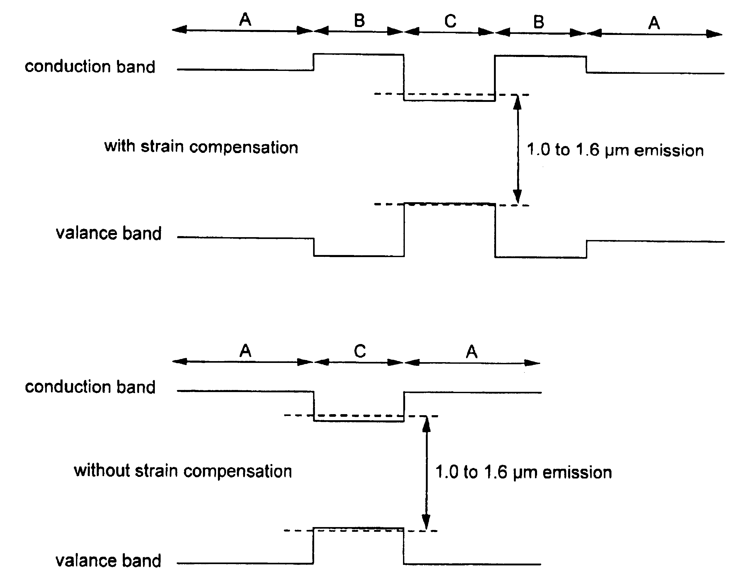
Through the use of strained InwGa1-wNxPyAszSb1-x-y-z / AlpGa1-pAs / GaAs heterostructures, the present invention's material system comprises: 1) Compressively strained InwGa1-wNxPyAszSb1-x-y-z quantum wells and tensile strained AlqGa1-qNrPsAs1-r-s barrier layers with a type-I band alignment; and 2) Compressively strained quantum wells utilizing multiple InwGa1-wNxPyAszSb1-x-y-z / InaGa1-aNbAs1-b layers with a type-II band alignment and tensile strained AlqGa1-qNrPsAs1-r-s barrier layers. Both material systems are grown pseudomorphically on GaAs substrates. As used herein, “pseudomorphic” shall mean having a sufficiently low density of misfit dislocations allowing for the production of lasers having sufficiently long lifetimes. Both type-I and type-II band-edge alignments are utilized in the present invention.

Light emission or absorption at wavelengths 1.0 μm to 1.6 μm are achieved by the present invention by using single or multiple combinations of active materials grown on material A, wi...


PUM


Abstract

The invention discloses improved structures of light-processing (e.g. light-emitting and light-absorbing/sensing) devices, in particular Vertical Cavity Surface Emitting Lasers (VCSELs), such as may find use in telecommunications applications. The disclosed VSCAL devices and production methods provide for an active region having a quantum well structure grown on GaAs-containing substrates, thus providing processing compatibility for light having wavelength in the range 1.0 to 1.6 μm. The active region structure combines strain-compensating barriers with different band alignments in the quantum wells to achieve a long emission wavelength while at the same time decreasing the strain in the structure. The improved functioning of the devices disclosed results from building them with multicomponent alloy layers having a large number of constituents. The invention discloses as a key constituent in the proposed alloy layers for the active region a substance, such as nitrogen (N), suitable for reducing bandgap energy (i.e., increasing light wavelength) associated with the layers while at the same time lowering the lattice constant associated with the structure and hence lowering strain.

Description

Vertical-cavity surface-emitting lasers (VCSELs) operating at 1.3 μm and 1.5 μm are desirable for low cost optical telecommunication systems and data links. Realization of these devices may enable digital communications applications such as “fiber to the home,” which operate over distances of only a few kilometers. Whereas lasers operating at a wavelength 1.3 μm are interesting for high-speed communication since they operate at the dispersion minimum of optical fibers, lasers at 1.55 μm are interesting for communications over larger distances as they transmit in the absorption minimum. Also, long-wavelength lasers have a low operating voltage, which makes them attractive for integration with integrated Si-based circuitry in which the trend has been toward lower and lower operating voltages with higher integration density. Due to the potentially-large market for 1.3 and 1.5 μm VCSELs, much research has been carried out to develop devices using different approaches based primarily on ...

Claims


Application Information

Patent Timeline
IPC IPC(8): H01L29/02H01L29/06H01S5/00H01L31/0304H01L31/0352H01L33/00H01S5/183H01S5/323H01S5/34H01S5/343
CPCB82Y10/00B82Y20/00H01L31/03046H01L31/035236H01S5/3434H01S5/183H01S5/32366Y02E10/544H01S5/3406H01S5/3422H01S5/34306Y02B10/10H01S5/3403
Inventor JOHNSON, SHANEDOWD, PHILIPBRAUN, WOLFGANGZHANG, YONG-HANGGUO, CHANG-ZHI
Owner THE ARIZONA BOARD OF REGENTS ON BEHALF OF THE UNIV OF ARIZONA
Why Eureka
Try Eureka