Semiconductor device, manufacturing method therefor, and semiconductor manufacturing apparatus

a semiconductor and manufacturing method technology, applied in the direction of instruments, gel state, crystal growth process, etc., can solve the problems of suppressing transistor characteristics, difficult to form uniformly a p-si film, and many defects in the crystal grain boundaries, etc., and achieve high mobility

Inactive Publication Date: 2005-03-01
UNIFIED INNOVATIVE TECH
View PDF14 Cites 25 Cited by
  • Summary
  • Abstract
  • Description
  • Claims
  • Application Information

AI Technical Summary

Benefits of technology

[0011]It is an object of the present invention to provide semiconductor devices including TFTs in which the transistor characteristics of the TFTs are made uniform at a high level, and the mobil

Problems solved by technology

It is difficult to form uniformly a p-Si film large in crystal grain size in a large area.
In addition, the crystal grain b

Method used


Image

  • Semiconductor device, manufacturing method therefor, and semiconductor manufacturing apparatus
  • Semiconductor device, manufacturing method therefor, and semiconductor manufacturing apparatus
  • Semiconductor device, manufacturing method therefor, and semiconductor manufacturing apparatus

Examples


third embodiment

[0064]FIG. 26 are schematic views showing irradiation systems of DPSS lasers used in modifications of the third embodiment;

fourth embodiment

[0065]FIG. 27 is a schematic view showing the principal part of a DPSS laser device according to the present invention;

[0066]FIG. 28 is a schematic view showing an example of arrangement of TFTs in a pixel region;

[0067]FIG. 29 is a schematic view showing the principal part of a DPSS laser device according to modification 2 of the fourth embodiment;

[0068]FIG. 30 is a schematic view showing the principal part of a DPSS laser device according to modification 3 of the fourth embodiment;

[0069]FIG. 31 is a schematic view showing the principal part of a DPSS laser device according to modification 4 of the fourth embodiment;

[0070]FIG. 32 is a graph showing a result obtained by examining the distribution of hydrogen in a buffer layer made of SiN or SiON, and a Si layer;

[0071]FIG. 33 is a photomicrographic view showing a state of an a-Si film peeling off;

[0072]FIG. 34 is a schematic sectional view showing a state that an a-Si film is formed over a glass substrate with a buffer layer being int...

first embodiment

[0077](First Embodiment)

[0078]Crystallization by Energy Beam Output Continuously along Time Axis

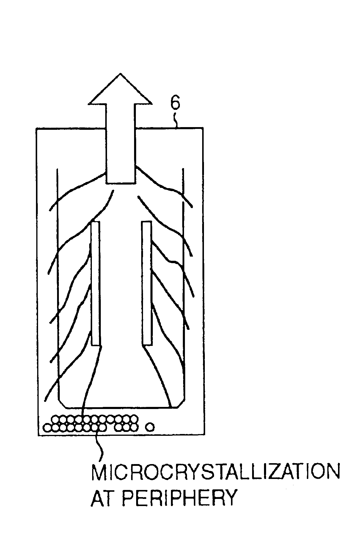
[0079]The principal part of the first embodiment of the present invention, i.e., crystallization of a semiconductor film using an energy beam which outputs energy continuously along the time axis, e.g., a solid state laser (DPSS (Diode Pumped Solid State Laser) laser) of semiconductor excitation (LD excitation) will be disclosed.

[0080]An energy beam continuous along the time axis can irradiate and scan, e.g., an amorphous silicon (a-Si film) to form large-size polysilicon crystals. The crystal grain size at this time is about several μm, and very large crystals can be formed. This crystal grain size is 10 to 100 times the size obtained by using a currently available excimer laser. Hence, such crystals are very advantageous to TFTs at a peripheral circuit portion required to operate at high speed.

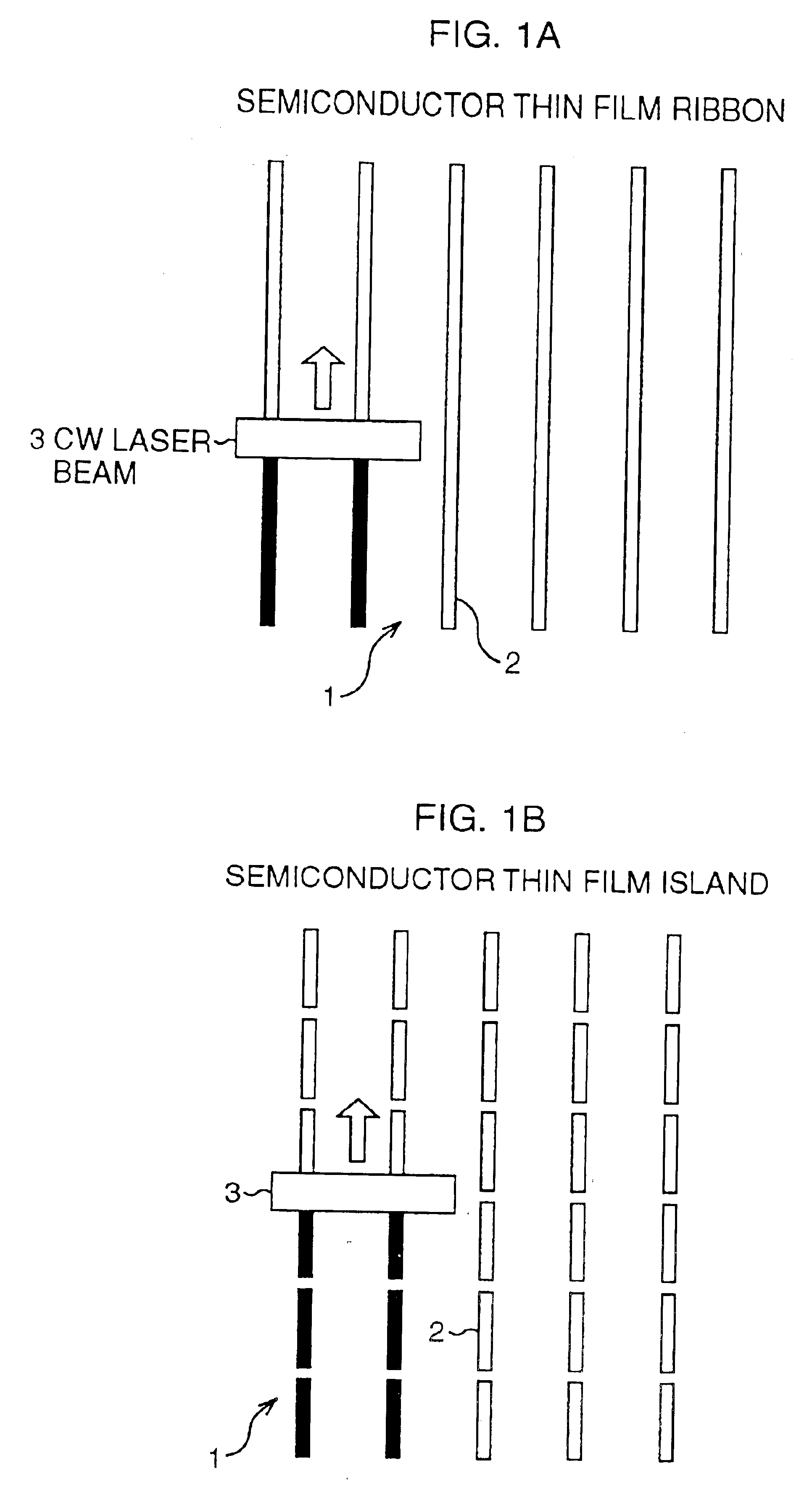
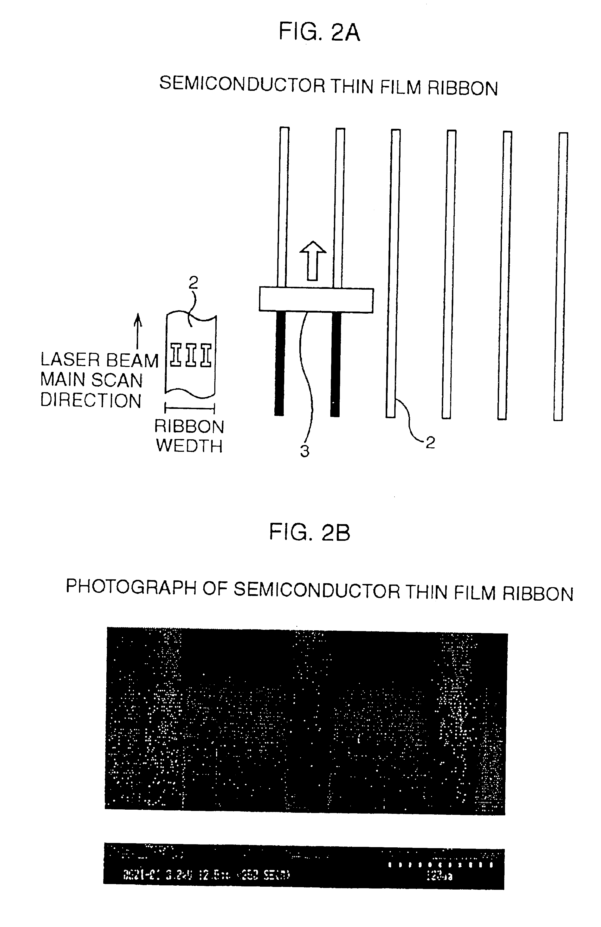
[0081]As shown in FIGS. 1A to 2B, an a-Si film 2 is patterned into a linear (ribbon) shape (FI...


PUM


Abstract

An a-Si film is patterned into a linear shape (ribbon shape) or island shape on a glass substrate. The upper surface of the a-Si film or the lower surface of the glass substrate is irradiated and scanned with an energy beam output continuously along the time axis from a CW laser in a direction indicated by an arrow, thereby crystallizing the a-Si film. This implements a TFT in which the transistor characteristics of the TFT are made uniform at high level, and the mobility is high particularly in a peripheral circuit region to enable high-speed driving in applications to a system-on glass and the like.

Description

CROSS-REFERENCE TO RELATED APPLICATIONS[0002]This application is a divisional of U.S. application with Ser. No. 09 / 935,090, filed Aug. 22, 2001 now U.S. Pat. No. 6,737,672.[0003]This application is based upon and claims priority of Japanese Patent Application Nos. 2000-255646 and 2001-202730, filed on Aug. 25, 2000 and Jul. 3, 2001, the contents being incorporated herein by reference.BACKGROUND OF THE INVENTION[0004]1. Field of the Invention[0005]The present invention relates to semiconductor devices, manufacturing methods of the same, and semiconductor manufacturing apparatus, in particular, for being suitably applied to a so-called system-on panel, in which a pixel region including thin film transistors and a peripheral circuit region including thin film transistors are formed on a non-crystallized (amorphous) substrate such as a non-alkali glass substrate.[0006]2. Description of the Related Art[0007]A TFT (Thin Film Transistor) is formed on a very thin, fine active semiconductor ...

Claims


Application Information

Patent Timeline
IPC IPC(8): H01L21/20H01L29/786H01L21/02H01L29/66H01L21/336G02F1/1345G02F1/136H01L21/268
CPCH01L21/2026H01L29/66757H01L29/78675H01L27/1281H01L27/1285H01L29/78696Y10T117/10Y10S117/904H01L21/02422H01L21/02488H01L21/02532H01L21/02595H01L21/02678H01L21/02683H01L21/02691G02F1/136
Inventor HARA, AKITOTAKEUCHI, FUMIYOYOSHINO, KENICHISASAKI, NOBUO
Owner UNIFIED INNOVATIVE TECH
Why Eureka
Try Eureka