Electron beam detector, scanning type electron microscope, mass spectrometer, and ion detector

a scanning electron microscope and detector technology, applied in the direction of material analysis using wave/particle radiation, optical radiation measurement, particle separator tube details, etc., can solve the problem of insufficient response of any of these fluorescent materials, and achieve the effect of preventing the deterioration of these components, good accuracy, and quick respons

Inactive Publication Date: 2005-03-01
HAMAMATSU PHOTONICS KK
View PDF34 Cites 25 Cited by
  • Summary
  • Abstract
  • Description
  • Claims
  • Application Information

AI Technical Summary

Benefits of technology

Preferably, the photodetector is a photomultiplier tube, and the fluorescence emitting surface of the compound semiconductor substrate is connected to a light incident window of the photomultiplier tube through the connecting means. By using a photomultiplier tube, it is possible to detect weak intensity electron beams with good accuracy. In this case, the photomultiplier tube preferably includes: a wall section forming a vacuum space with the light incident window, a photocathode formed in the vacuum space on an inner surface of the light incident window, and an electron multiplying section and an anode formed in the vacuum space. The photocathode generates electrons in response to incident fluorescence from the compound semiconductor substrate, the electron multiplying section multiplies the electrons, and the anode collects the multiplied electrons. The photocathode, the electron multiplying section, and the anode are not exposed to the atmosphere, even when the electron beam detector is removed from the vacuum chamber used for detecting electron beams, since they are formed inside the vacuum space. Accordingly, it is possible to use the electron beam detector for different applications, while preventing the deterioration of these components. It is preferable that the electron multiplying section includes a plurality of stacked dynodes. The above stacked-type electron multiplying section exhibits a quick response. Therefore, electron multiplying section can detect electron beams with very quick response when integrated with the highly responsive compound semiconductor substrate.
Alternatively, the photodetector may include an avalanche photodiode. In this case, the fluorescence emitting surface of the compound semiconductor substrate is connected to the light incident surface of the photodetector through the connecting means. By using the avalanche photodiode described above, it is possible to detect weak intensity electron beams with good accuracy. It is preferable that the connecting means guides fluorescence to the light incident surface of the photodetector, tapering an output surface thereof, when the light incident surface of the photodetector is smaller than the fluorescence emitting surface of the compound semiconductor substrate. In this case, the connecting means includes a light guide. The light guide preferably has a fluorescence input surface connected to the fluorescence emitting surface of the compound semiconductor substrate, and a fluorescence output surface connected to the light incident surface of the photodetector, the fluorescence output surface being smaller than the fluorescence input surface. Since an avalanche photodiode having a small light incident surface and exhibiting quick good response can be used, it is possible to detect electron beams with good response. Moreover, since the fluorescent light is transmitted while reducing the fluorescence output surface area, it is possible to use a compound semiconductor substrate having a large surface area. Therefore, an electron beam can be received in a large surface area and detected on a one-time basis, which improves the detection accuracy of the photodetector.

Problems solved by technology

However, a sufficient response has not been achieved with any of these fluorescent materials.

Method used


Image

  • Electron beam detector, scanning type electron microscope, mass spectrometer, and ion detector
  • Electron beam detector, scanning type electron microscope, mass spectrometer, and ion detector
  • Electron beam detector, scanning type electron microscope, mass spectrometer, and ion detector

Examples


first embodiment

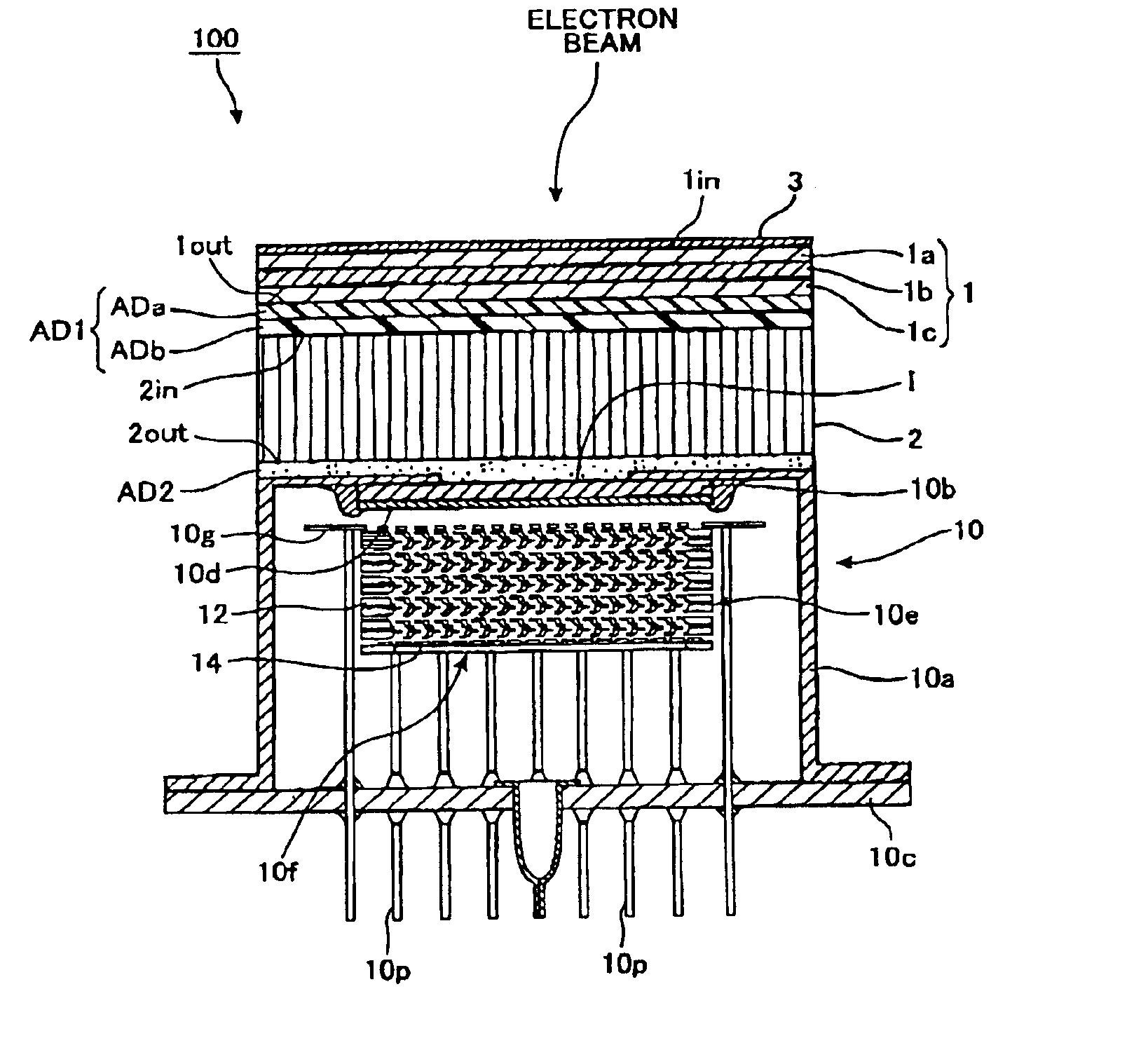
FIG. 1 is a vertical cross-sectional view showing an electron beam detector 100 according to a first embodiment.

The electron beam detector 100 has a substantially cylindrical shape and includes a compound semiconductor substrate 1, a light guide 2, and a photomultiplier tube 10 as the photodetector arranged in the axial direction of the electron beam detector 100, these components being formed integrally. The compound semiconductor substrate 1 functions to convert incident electrons into fluorescent light. The photomultiplier tube 10 has a light incident surface I and functions to detect light incident on the light incident surface I. The light guide 2 is an optical member formed of a fluorescent light transmissive material. The light guide 2 is fixed to the light incident surface I of the photomultiplier tube 10. The compound semiconductor substrate 1 is mounted on the light guide 2. In this way, the compound semiconductor substrate 1 is optically coupled with the light incident su...

second embodiment

FIG. 7 is a vertical cross-sectional view showing the electron beam detector 100 according to a second embodiment. The electron beam detector 100 of the present embodiment differs from that of the first embodiment only in that the compound semiconductor substrate 1 of the present embodiment includes only the substrate layer 1c formed of an AlGaAsP compound semiconductor material and the light-emitting layer 1b formed of a GaAsP compound semiconductor material that is formed on the substrate layer 1c.

The GaAsP compound semiconductor material is a single crystal that generates fluorescent light in response to incident electron beams. The wavelength of light emitted from the GaAsP is 720 nm. As in the first variation of the first embodiment, the compound semiconductor substrate 1 of the present embodiment does not include the coating layer 1a, and the metal layer 3 is provided directly on the light-emitting layer 1b. Therefore, the surface of the light-emitting layer 1b (the top surfa...

third embodiment

FIG. 9 is a vertical cross-sectional view showing the electron beam detector 100 according to a third embodiment. The electron beam detector 100 of the present embodiment differs from that of the first embodiment only in that the adhesive layer AD1 is constructed of a single layer formed of a fluorescent light transmissive adhesive (synthetic resin) rather than two layers. The adhesive layer AD1 having this single-layer construction affixes the compound semiconductor substrate 1 to the light guide 2. With this construction, the compound semiconductor substrate 1 and light guide 2 can be connected with sufficient strength. Further, sufficient good response can be achieved.


PUM

PropertyMeasurementUnit
carrier concentrationaaaaaaaaaa
wavelengthaaaaaaaaaa
thicknessaaaaaaaaaa

Abstract

In an electron beam detector, a light guide optically couples a fluorescence emitting surface of the compound semiconductor substrate to a light incident surface of the photodetector, and physically connects the compound semiconductor substrate with the photodetector, thereby integrating the compound semiconductor substrate with the photodetector. When the compound semiconductor substrate converts incident electrons to fluorescent light, the light guide guides the fluorescent light to the photodetector, and the photodetector detects the fluorescent light, thereby detecting the incident electrons.

Description

TECHNICAL FIELDThe present invention relates to an electron beam detector, a scanning type electron microscope, a mass spectrometer, and an ion detector.BACKGROUND ARTConventional electron beam detectors measures the value of the current flow generated by the electron beam in order to measure high-intensity electron beams.However, an electron beam detector employed in a scanning type electron microscope, for example, produces little electric charge when the intensity of the electron beam is relatively weak. Therefore, secondary electrons generated from the surface of a sample irradiated by an electron beam are collected and irradiated onto a fluorescent material. A photomultiplier tube is used to measure the fluorescence emitted by the fluorescent material.Fluorescent materials well known in the art include CaF2, CaP5O14, P47, P46, YAG: Ce3+, YAP: Ce3+ (polycrystalline), and YAP: Ce3+ (single-crystal). However, a sufficient response has not been achieved with any of these fluorescen...

Claims


Application Information

Patent Timeline
Patent Type & Authority Patents(United States)
IPC IPC(8): H01J37/244H01J49/00H01J43/00H01J29/38H01J43/04H01J29/10
CPCH01J29/385H01J37/244H01J49/025H01J43/04H01J2237/28
Inventor KONDO, MINORUNAGAI, TOSHIMITSUKIBUNE, ATSUSHI
Owner HAMAMATSU PHOTONICS KK
Why Eureka
Try Eureka