Chip antenna, radio communications terminal and radio communications system using the same and method for production of the same

a radio communication terminal and antenna technology, applied in the direction of helical antennas, non-resonant long antennas, resonant antennas, etc., can solve the problems of mechanical strength, electrical performance, environment-resistance performance, mechanical strength, etc., and achieve the effect of simple structure, good antenna characteristic and small variation in antenna characteristi

Inactive Publication Date: 2005-03-01
PANASONIC CORP
View PDF16 Cites 17 Cited by
  • Summary
  • Abstract
  • Description
  • Claims
  • Application Information

AI Technical Summary

Benefits of technology

An object of the present invention is to provide a chip antenna that is simple in structure, demonstrates a good antenna characteristic, shows a significantly small variation in antenna characteristic between individual antennas, requires no circuit adjustments, is improved in its productivity, and is capable of being mounted on a circuit board, and a wireless terminal and a wireless communications system using the chip antenna, and a method of producing the chip antenna.
By virtue of the above described configuration, such a chip antenna can be realized that is simple in structure yet shows a good antenna characteristic, produces a significantly small variation in antenna characteristic between individual antennas, requires no circuit adjustments, is improved in its productivity, and is capable of being mounted on a circuit board.

Problems solved by technology

These antennas are complicated in structure and require a large number of component parts and further had problems with mechanical strength, electrical performance, and environment-resistive performance.
Thus, they have problems of complexity of structure, multiplicity of components, and production of variations in antenna characteristics among individual antennas leading to the requirement of circuit adjustments for absorbing the variations, and hence poor productivity of the antennas.

Method used


Image

  • Chip antenna, radio communications terminal and radio communications system using the same and method for production of the same
  • Chip antenna, radio communications terminal and radio communications system using the same and method for production of the same
  • Chip antenna, radio communications terminal and radio communications system using the same and method for production of the same

Examples


embodiment 1

<Embodiment 1>

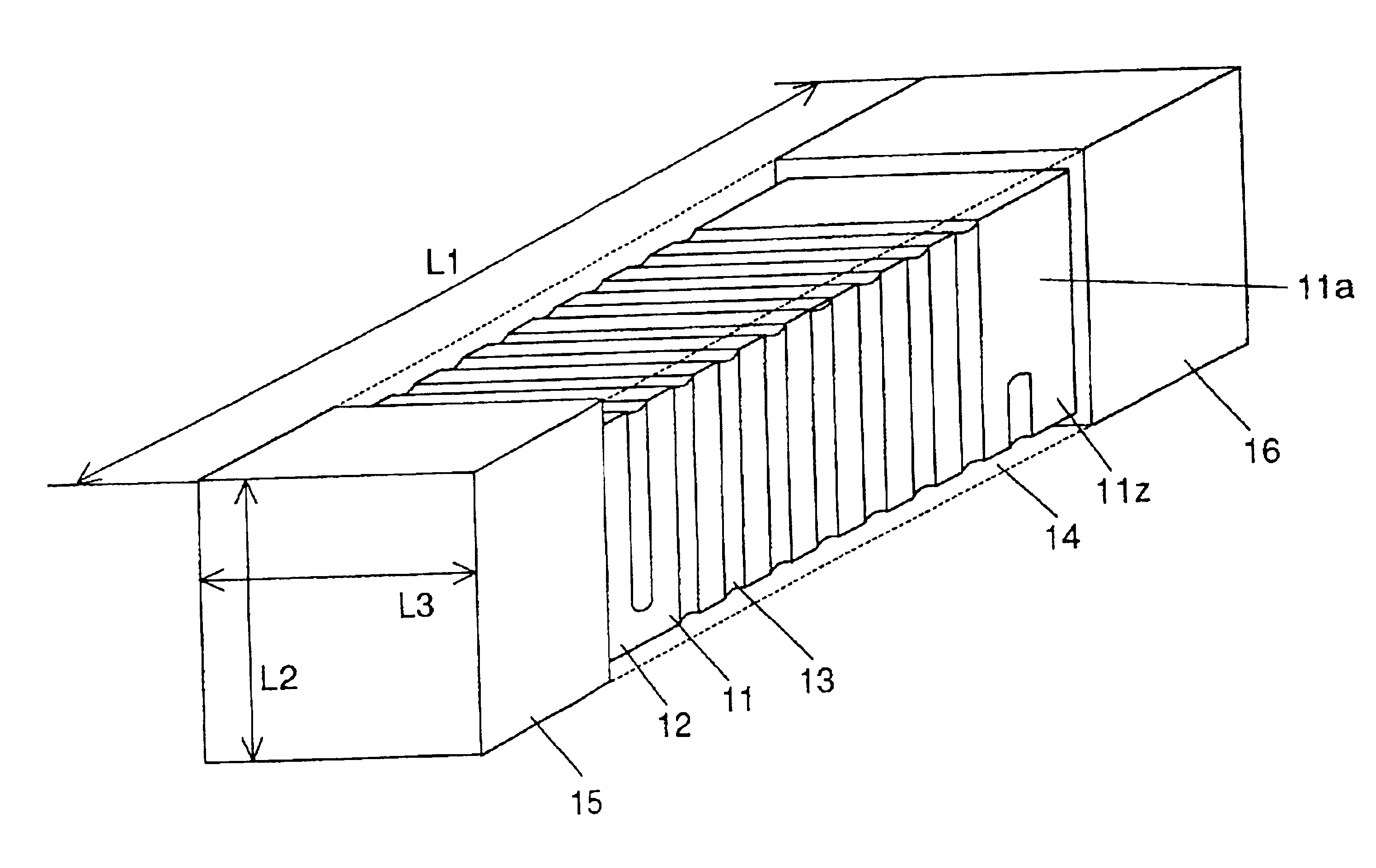
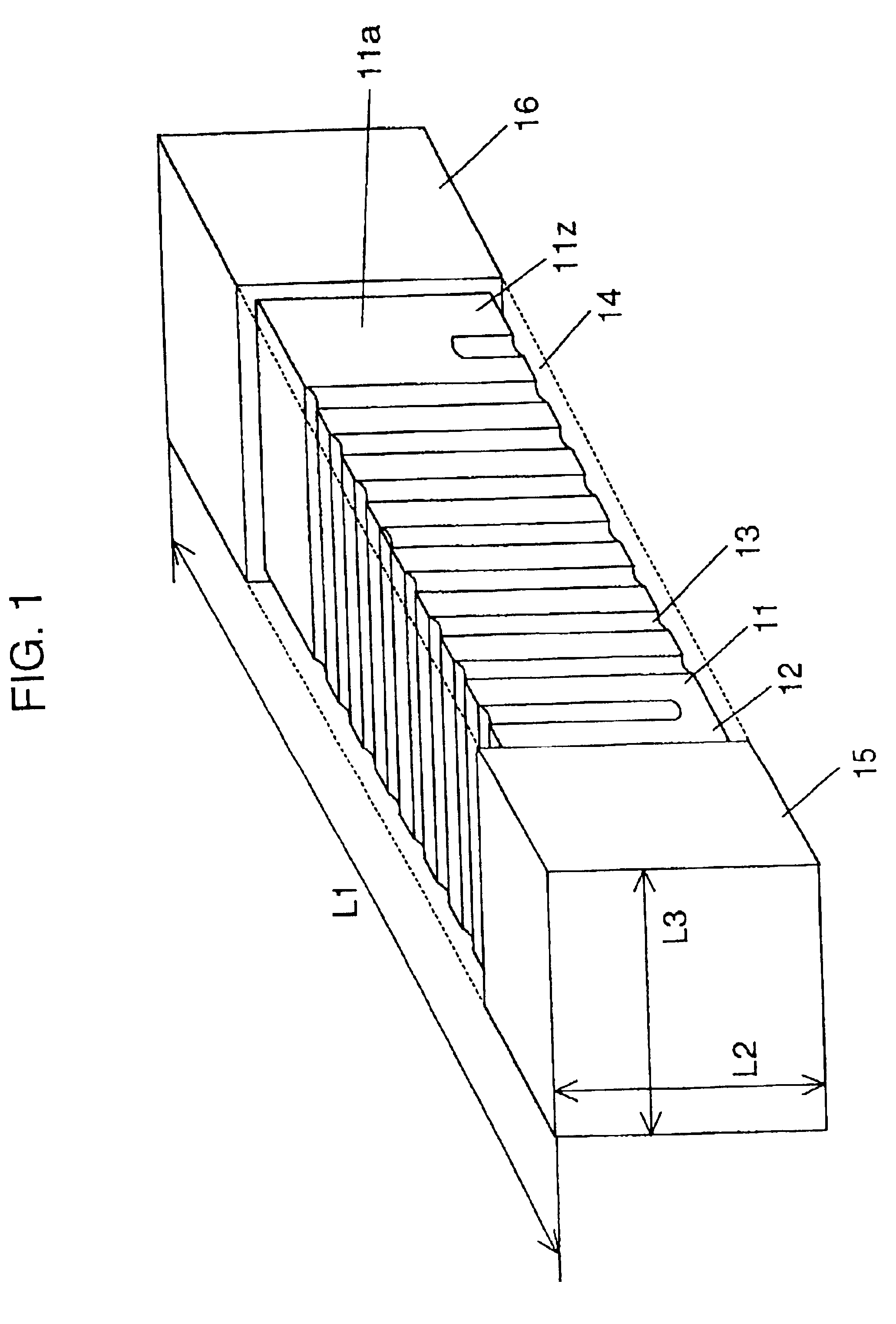
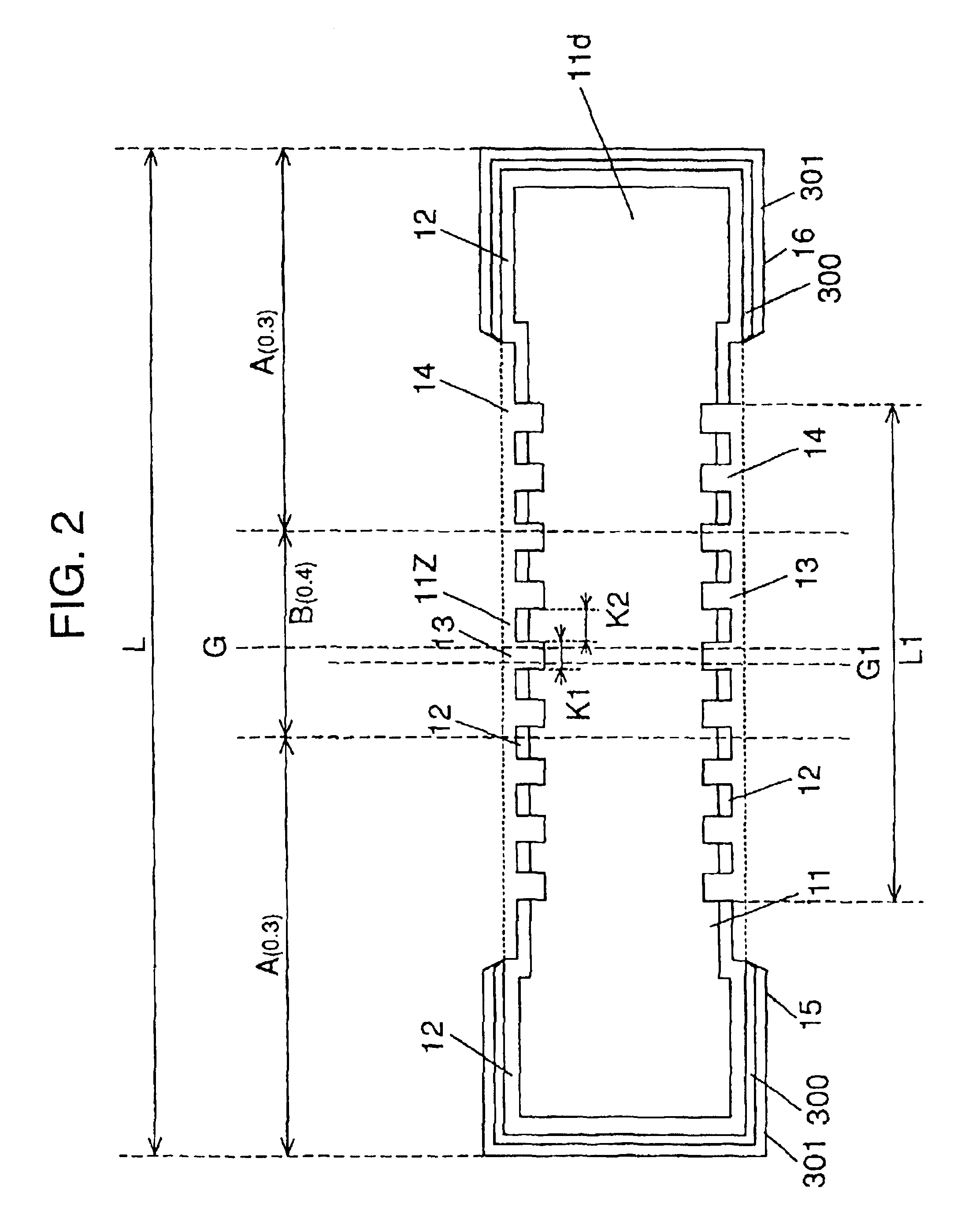
FIG. 1 and FIG. 2 are a perspective view and a side sectional view of a chip antenna in a preferred embodiment of the present invention, respectively. In FIG. 1, conductive film 12 in a helical shape is disposed on a side face of core body 11 of the chip antenna. Groove 13 in a helical shape is made in core body 11 and conductive film 12. Protection member 14 is provided on conductive film 12. Terminal portions 15 and 16 of the chip antenna each have a terminal electrode on an end face thereof

It is preferred that the chip antenna of the embodiment have operating frequency bands belonging to a microwave range of 0.7-7.0 GHz and have length L1, width L2, and depth L3 of the chip antenna as follows:L1=4.0-40.0 mm;L2=0.5-5.0 mm; andL3=0.5-5.0 mm.

When L1 is below 4.0 mm, the value of inductance becomes much smaller than required and it becomes impossible to obtain the antenna operation at a desired frequency range. When L1 is above 40.0 mm, the element itself becomes l...

embodiment 2

<Embodiment 2>

FIG. 6 is a side sectional view of a chip antenna showing embodiment 2 of the invention. The point of this embodiment that is different from embodiment 1 is in the protection member of the conductive film. In this embodiment, differing from polymeric material such as resin used in embodiment 1, a metallic film or the like is used as the protection member 14b as shown in FIG. 6. In this case, protection member 14b shown in FIG. 6 is formed of metallic material having good weather resistance. The material is constituted of at least one material selected from a material group of gold, platinum, palladium, silver, tungsten, titanium, nickel, and tin, or an alloy material of a material selected from the above material group and element not belonging to the material group. Especially from the point of view of cost and weather resistance, gold or gold alloy, or tin and tin alloy (excluding tin-lead alloy) is preferred. Protection member 14b may preferably be formed by pl...

embodiment 3

<Embodiment 3>

FIG. 7 is a side sectional view of a chip antenna showing embodiment 3 of the invention. The point of this embodiment that is different from embodiment 1 is in the protection member of the conductive film on the chip antenna.

When a coated resin material is used as the protection member, as shown in FIG. 2, or protection member 14 formed by electrolytic deposition is used, a great variation in the antenna characteristics may sometimes occur. More specifically, when a resin material having a certain value of dielectric constant is present in groove 13, it causes a variation in the antenna characteristics. The variation in the antenna characteristics will be suppressed if the quantity of the resin material entering groove 13 can be controlled but it is a difficult task in mass production. Thus, when epoxy resin or the like is applied to the antenna element portion, the quantity of resin entering groove 13 differs from chip antenna to chip antenna. The antenna charact...


PUM


Abstract

A chip antenna that is simple in structure, produces small variation in antenna characteristics between individual antennas, and requires no circuit adjustments, is excellent in productivity. The chip antenna is capable of being mounted on a circuit board, as well as a wireless terminal using the chip antenna. A method of fabricating the chip antenna. A core body is made from an insulating material in a quadrangular or circular cylinder shape. A conductor in a helical shape is mounted on the side surface of the core body. A terminal portion is provided on the core body and electrically connected with an end portion of the conductor. The width, depth, and length of the core body are within ranges of 0.5-5 mm, 0.5-5 mm, and 4-40 mm, respectively. Intrinsic volume resistance and relative dielectric constant of the material are 1013 Ω·m or above and 40 or below, respectively.

Description

FIELD OF THE INVENTIONThe present invention relates to a chip antenna to be mounted on a circuit board of electronic apparatus for carrying out wireless communications such as mobile communications, a wireless terminal using the same, and a method for production of the same.BACKGROUND OF THE INVENTIONWith rapid development in mobile communications, radio terminal equipment represented by mobile telephones are springing into wide use.The development owes greatly to advancement in high-frequency integrated circuit technology and development of smaller, lighter, and higher-performance antennas. As an example of such an antenna, a helical antenna produced by forming a helical conductor on an insulating rod is disclosed in Japanese Patent Laid-open Publication No. 10-65432 (1998). Although this antenna is being used as a substitute for a whip-type (rod-shaped) antenna and contributing to the provision of a smaller and lighter antenna, it is of a type used by being projected outward from ...

Claims


Application Information

Patent Timeline
Patent Type & Authority Patents(United States)
IPC IPC(8): H01Q1/38H01Q1/36H01Q11/08H01Q1/24H01Q11/00
CPCH01Q1/243H01Q11/08H01Q1/38H01Q1/362
Inventor YOSHINOMOTO, MAKOTOSAKITA, HIROMIISOZAKI, KENZOSHIIBA, KENGOGOTO, KAZUHIDEKANMERA, MITSUOKUROKI, MASANOBUSASAKI, KATSUMI
Owner PANASONIC CORP
Why Eureka
Try Eureka