Microfabricated apertures for supporting bilayer lipid membranes

a technology of bilayer lipid membranes and microfabricated apertures, which is applied in the direction of diaphragms, immobilised enzymes, electrolysis, etc., can solve the problems of uniform manufacture, inability to generally form features smaller than 0.5 m, and inability to stabilize albms as membranes found, etc., to achieve greater control over experimental parameters, design simplicity, and the effect of greater control

Inactive Publication Date: 2005-03-08
THE BOARD OF TRUSTEES OF THE LELAND STANFORD JUNIOR UNIV
View PDF11 Cites 149 Cited by
  • Summary
  • Abstract
  • Description
  • Claims
  • Application Information

AI Technical Summary

Benefits of technology

[0022]The methods, devices and systems of the invention provide multiple advantages. Advantages over other silicon-based substrates include simplicity of design and the bilayer formation technique. The present methods for treating silicon substrates so as to provide hydrophobic silicon substrate surfaces and for forming nanoapertures in them provides for the use of the Langmuir-Blodgett technique for forming ALBMs on silicon substrates. ALBMs formed by the methods and with the devices of the invention are more stable and reproducible than membranes formed using prior techniques and devices. In addition, due at least in part to the greater control over the design and manufacturing of apertures and reservoirs, the present invention provides greater control over experimental parameters than prior methods and devices.

Problems solved by technology

However, features smaller than about 0.5 μm cannot generally be formed by these techniques.
ALBMs are not as stable as membranes found in living cells.
In addition, ALBMs are formed across artificial apertures, which may have discontinuities and defects at the edges and surfaces and which are typically formed by manual processes which preclude uniformity of manufacture.
In addition, where a biosensor depends upon a membrane-bound biomolecule as a sensor element, instability or rupture of the membranes destroys the sensor element.

Method used


Image

  • Microfabricated apertures for supporting bilayer lipid membranes
  • Microfabricated apertures for supporting bilayer lipid membranes
  • Microfabricated apertures for supporting bilayer lipid membranes

Examples


example 1

Microfabrication of Apertures

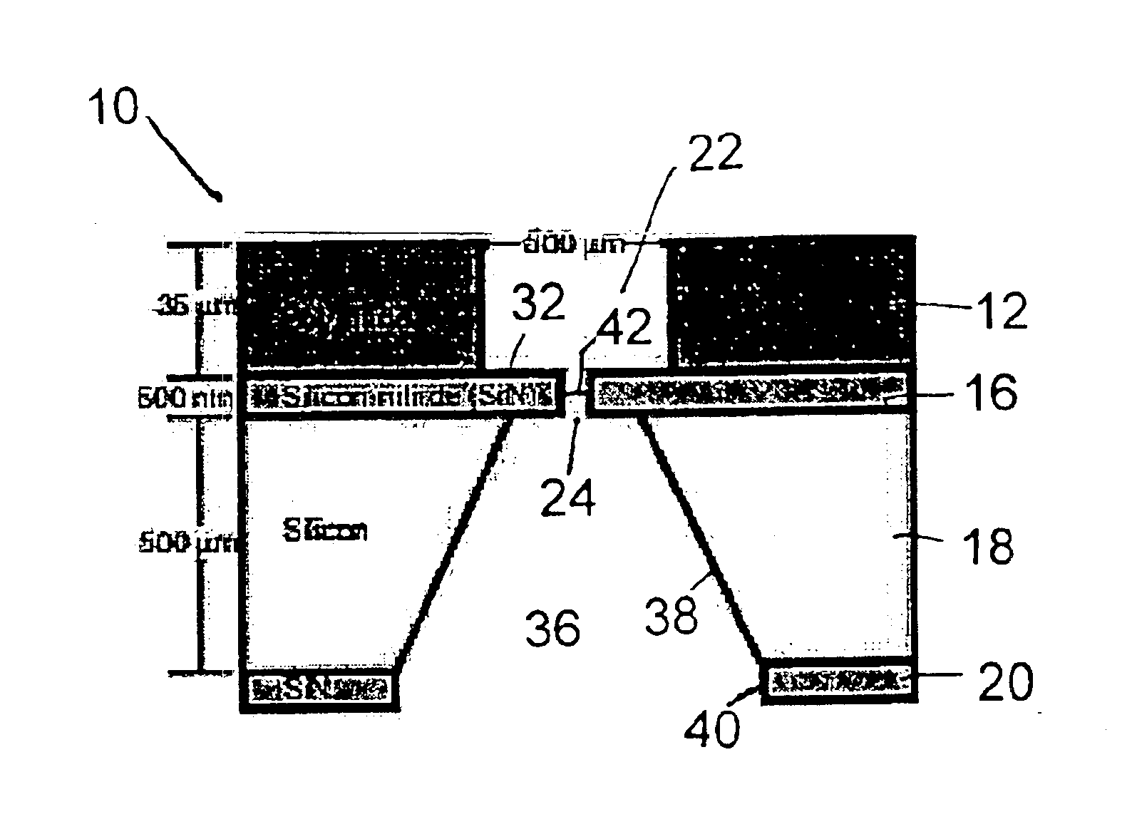
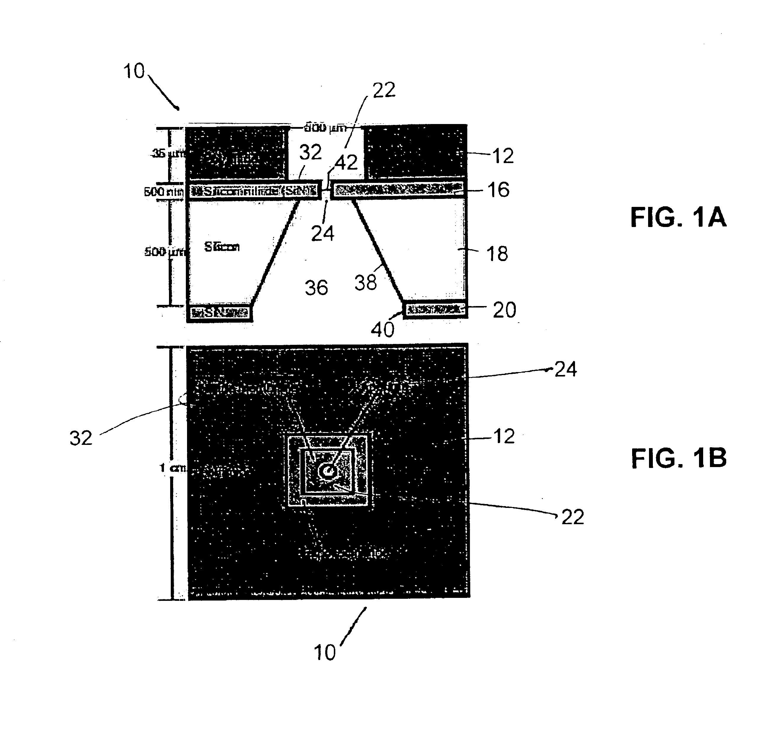
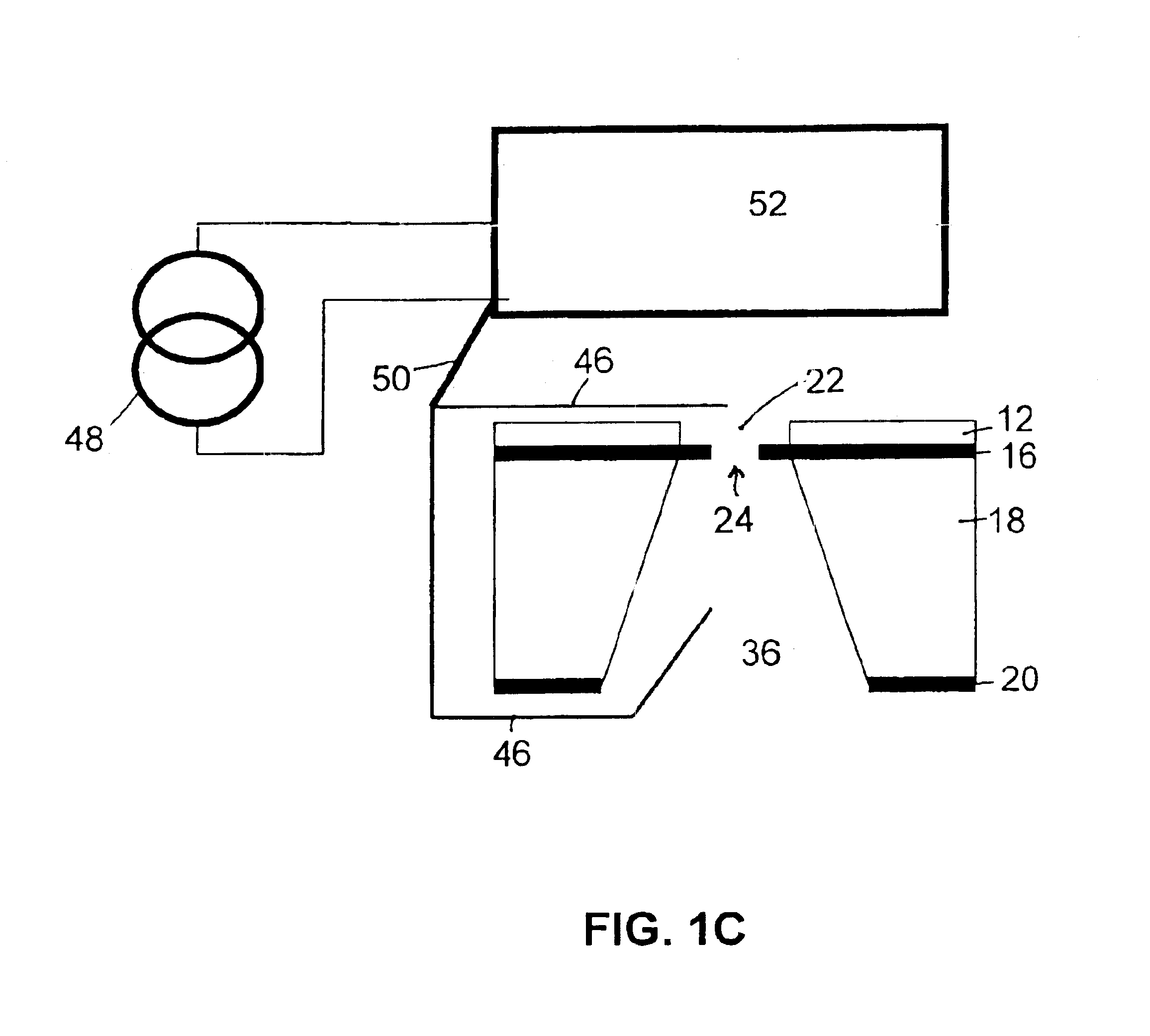
[0050]Microfabricated apertures on a silicon chip surfaces have been made using the Stanford Nanofabrication Facility. Microfabricated wells with microfabricated apertures are shown in FIG. 2. Silicon processing techniques were adapted for producing micrometer and nanometer-sized apertures in a silicon nitride membrane (large features and small features). Using low-pressure chemical vapor deposition (LPCVD), a thin layer (500 nm) of silicon nitride was grown on the surface of orientation silicon wafers. A combination of lithography to define the structures in a photosensitive polymer was followed by plasma etching to pattern the structures in the silicon nitride-created apertures on one side of the wafer and an etchant masking layer on the other side. An anisotropic etchant, such as tetramethylammonium hydroxide (TMAH), was used to remove the silicon along the {111} crystal plane, but leave the silicon nitride unaffected. This produced a via hole (a con...

example 2

Device Fabrication and Optimization

[0059]This Example describes the manufacture and optimization of devices embodying features of the invention for use in forming bilayer membranes across the microfabricated apertures of the devices. Nanoaperture chips were made with surface areas of about 1 cm2 and with a final thickness of roughly 0.5 mm. Circular apertures of 25 μm through 250 μm (diameter) were plasma etched in 500 nm thick silicon nitride. The chips were covered in a thick polyimide, except for a square region of exposed silicon nitride 500 μm on a side.

[0060]Fabrication was done at the Stanford Nanofabrication Facility (SNF) with 4 inch, orientation, boron-doped, double-polished silicon wafers, nominally 500 μm thick. Using low-pressure chemical vapor deposition (LPCVD), a thin layer (500 nm) of silicon nitride was grown on the surface of the wafers. Standard contact photolithography and plasma etching of the silicon nitride was used to define the small features (e.g., the ap...

example 3

Substrates with Multiple Nanoapertures

[0069]The techniques described in the previous example may also be used to produce silicon substrates having more than one nanoaperture. Multiple nanoapertures may be formed within a single recess on a substrate, or multiple assemblies each having a single or multiple nanoapertures within a single recess may be formed on a substrate.

[0070]A 4 inch, orientation, boron-doped, double-polished silicon wafer, nominally 500 μm thick, was used to form a nanoaperture chip having multiple nanoapertures within a single recess. Using low-pressure chemical vapor deposition (LPCVD), a thin layer (500 nm) of silicon nitride was grown on the surface of the wafer. Standard contact photolithography and plasma etching of the silicon nitride was used to define the small features (e.g., the apertures). One hundred twenty one 5 μm nano-apertures were formed in the wafer, in a square pattern having eleven nanoapertures on a side with the nanoapertures spaced 100 μm ...


PUM

PropertyMeasurementUnit
diameteraaaaaaaaaa
temperatureaaaaaaaaaa
diameteraaaaaaaaaa

Abstract

The invention provides microfabricated silicon substrates and devices having extremely small apertures (termed “nanoapertures”) and methods for producing such nanoapertures. The devices have a nanoaperture (which may have a diameter ranging from about a few millimeters to as small as a few nm) across a substrate effective to connect two regions separated by the substrate. The devices are suitable for the formation of lipid bilayer membranes across the apertures, and for use in devices such as biosensors. Substrates and devices may include multiple nanoapertures, which may each support a lipid bilayer membrane, allowing fault tolerant devices such as fault-tolerant biosensors, and allowing devices able to sense more than one target molecule.

Description

CROSS REFERENCES[0002]This application claims priority from and incorporates by reference in its entirety U S. Provisional Application Ser. No. 60 / 301,972, titled “Microfabricated Apertures For Supporting Bilayer Lipid Membranes”, by David Bloom et al., filed Jun. 29, 2001.FIELD OF THE INVENTION[0003]The invention pertains to microfabricated apertures, methods for forming microfabricated apertures, and devices having microfabricated apertures.BACKGROUND OF THE INVENTION[0004]Small-sized apertures find use in a variety of applications including scanning microscopes, ink-jet nozzles, and micromechanical systems. Small apertures are often made using microfabrication techniques. Microfabrication techniques and applications may be found, for example, in U.S. Pat. No. 5,517,280 to Quate, U.S. Pat. No. 5,858,256 to Minne et al., U.S. Pat. No. 5,943,075 to Lee et al., and U.S. Pat. No. 6,219,015 to Bloom. All patents, both supra and infra, are hereby incorporated by reference in their entir...

Claims


Application Information

Patent Timeline
Patent Type & Authority Patents(United States)
IPC IPC(8): B82B1/00B82B3/00B81B1/00
CPCB81B1/004G01N33/48721B81C1/00158B81B2201/0214B81B2203/0353
Inventor BLOOM, DAVID M.PETERMAN, MARK C.ZIEBARTH, JONATHAN M.
Owner THE BOARD OF TRUSTEES OF THE LELAND STANFORD JUNIOR UNIV
Why Eureka
Try Eureka