Suppressing the leakage current in an integrated circuit

a technology of integrated circuit and leakage current, which is applied in the direction of power consumption reduction, pulse technique, instruments, etc., can solve the problems of drop in operating speed, increase in leakage current, increase in power consumption due to leakage current reaches a level which cannot be achieved,

Inactive Publication Date: 2005-03-08
TEXAS INSTR INC
View PDF5 Cites 47 Cited by
  • Summary
  • Abstract
  • Description
  • Claims
  • Application Information

AI Technical Summary

Benefits of technology

Furthermore, a semiconductor integrated circuit of the present invention has a functional circuit which performs prescribed processing, a voltage supply circuit which supplies a first source voltage or a second source voltage higher than the aforementioned first source voltage according to a source voltage control signal, a transistor which is connected between the voltage supply terminal of the aforementioned voltage supply circuit and the voltage input terminal of the aforementioned functional circuit in order to control the power supplied to the aforementioned functional circuit according to a conduction control signal applied to its gate terminal, and a control circuit which supplies the aforementioned source voltage control signal and the aforementioned conductivity control signal; wherein, the aforementioned voltage supply circuit supplies the aforementioned second source voltage while the aforementioned functional circuit is in a standby status, and it supplies the aforementioned first source voltage while the aforementioned functional circuit is operating.
In addition, in the present invention, preferably, the aforementioned transistor is configured with an nMOS transistor, and the voltage level of the aforementioned conductivity control signal is lower than the source voltage of the aforementioned second source voltage when the aforementioned functional circuit is in the standby status.
In addition, in the present invention, preferably, a bias voltage applied to the channel region of the aforementioned transistor is equal to the aforementioned second source voltage or lower than the aforementioned second source voltage when the aforementioned functional circuit is in the standby status, and the aforementioned bias voltage is equal to the aforementioned first source voltage or higher than the aforementioned first source voltage when the

Problems solved by technology

When the source voltage drops and becomes close to threshold voltage Vth of a MOS transistor, a drop in its operating speed becomes a problem.
However, along with a decrease in the threshold voltage of the transistor is an increase in leakage current results.
Thus, while in a standby status, that is, when not operating, the increase in power consumption due to leakage current reaches a level which cannot be ignored, so that reduction of power consumption, the primary objective of reducing the voltage, can no longer be realized.
In the case of the aforementioned technology in which the leakage current path is cut off using a cut-off transistor during operation, it is difficult to assure the reliability of the gate oxide film in the cut-off transistor.

Method used


Image

  • Suppressing the leakage current in an integrated circuit
  • Suppressing the leakage current in an integrated circuit
  • Suppressing the leakage current in an integrated circuit

Examples


first embodiment

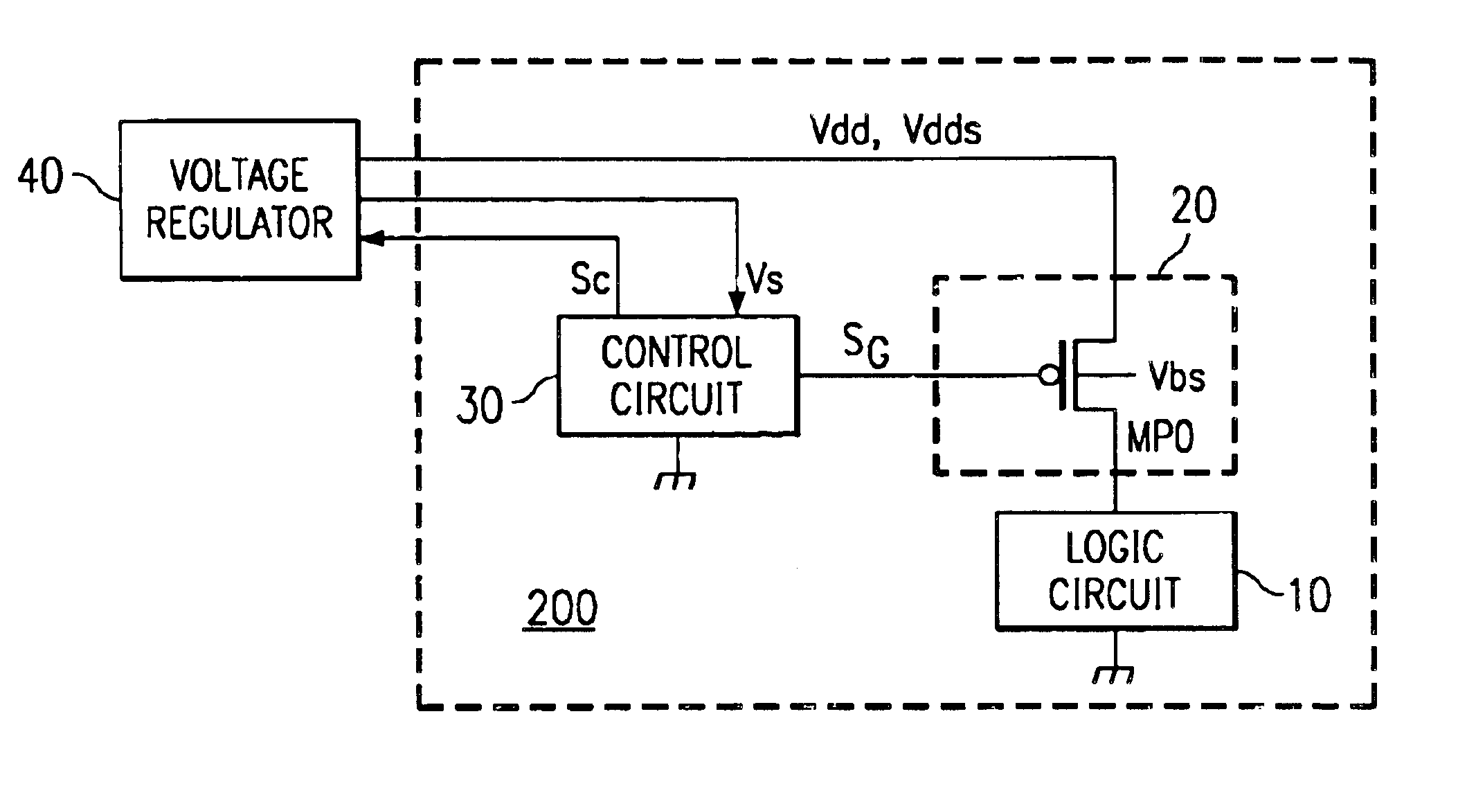
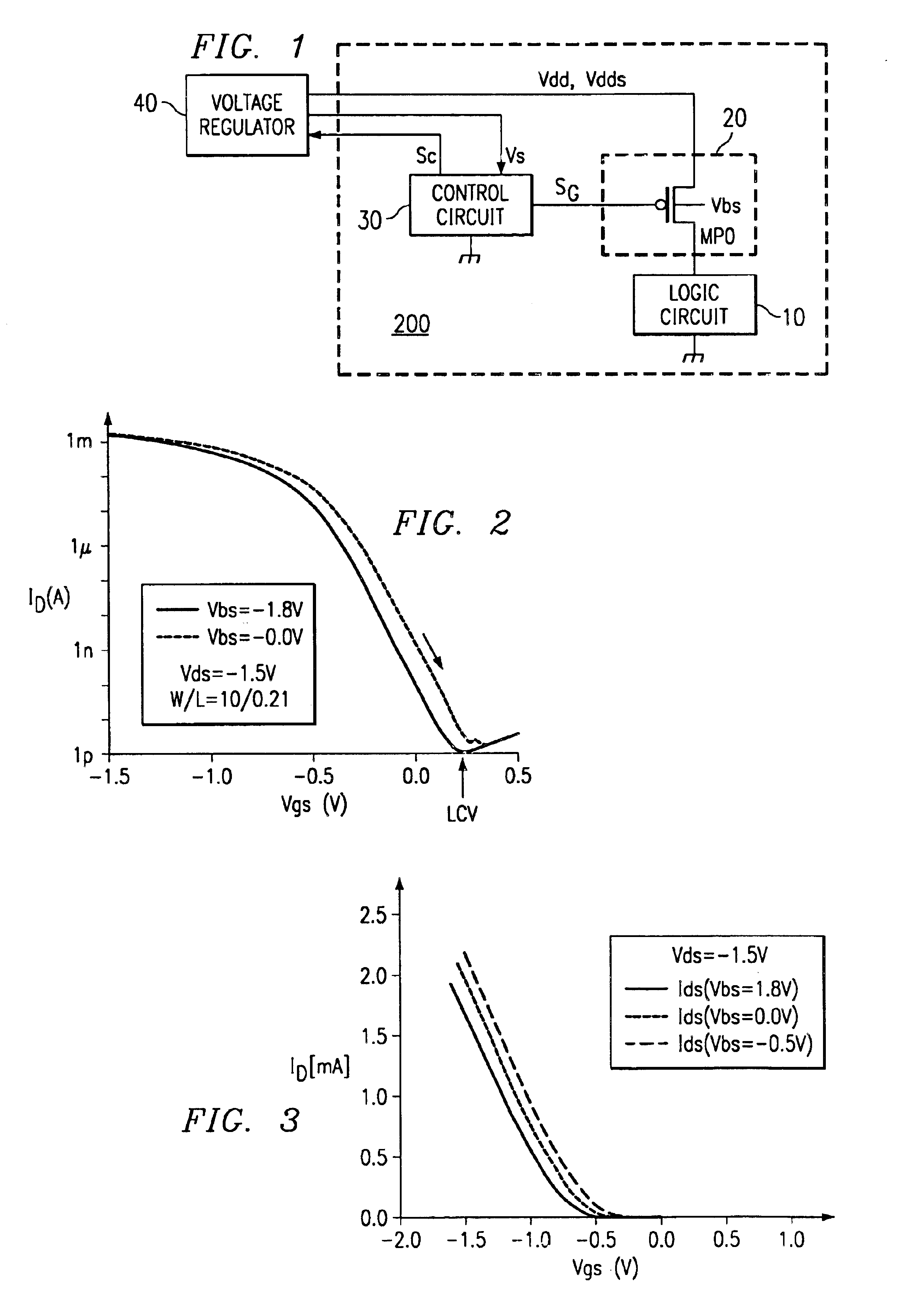
FIG. 1 is a circuit diagram showing a first embodiment of a semiconductor integrated circuit pertaining to the present invention.

As shown in the figure, the semiconductor integrated circuit of the present embodiment is configured with logic circuit 10 having a CMOS structure, switching circuit 20 for supplying an operating current to logic circuit 10, voltage regulator 40 capable of supplying variable and multiple voltages, and control circuit 30 for controlling voltage regulator 40.

In the case of the semiconductor integrated circuit of the present embodiment, reduction in the leakage current is realized by taking advantage of the characteristic that when gate-source voltage Vgs of a MOS transistor is kept at a specific value, leakage current of said transistor is at the lowest value. Furthermore, the phenomenon that a minimum value is present in the leakage current according to gate-source voltage Vgs is referred to as LCV (Leakage Current Valley: valley in the leakage current).

As ...

second embodiment

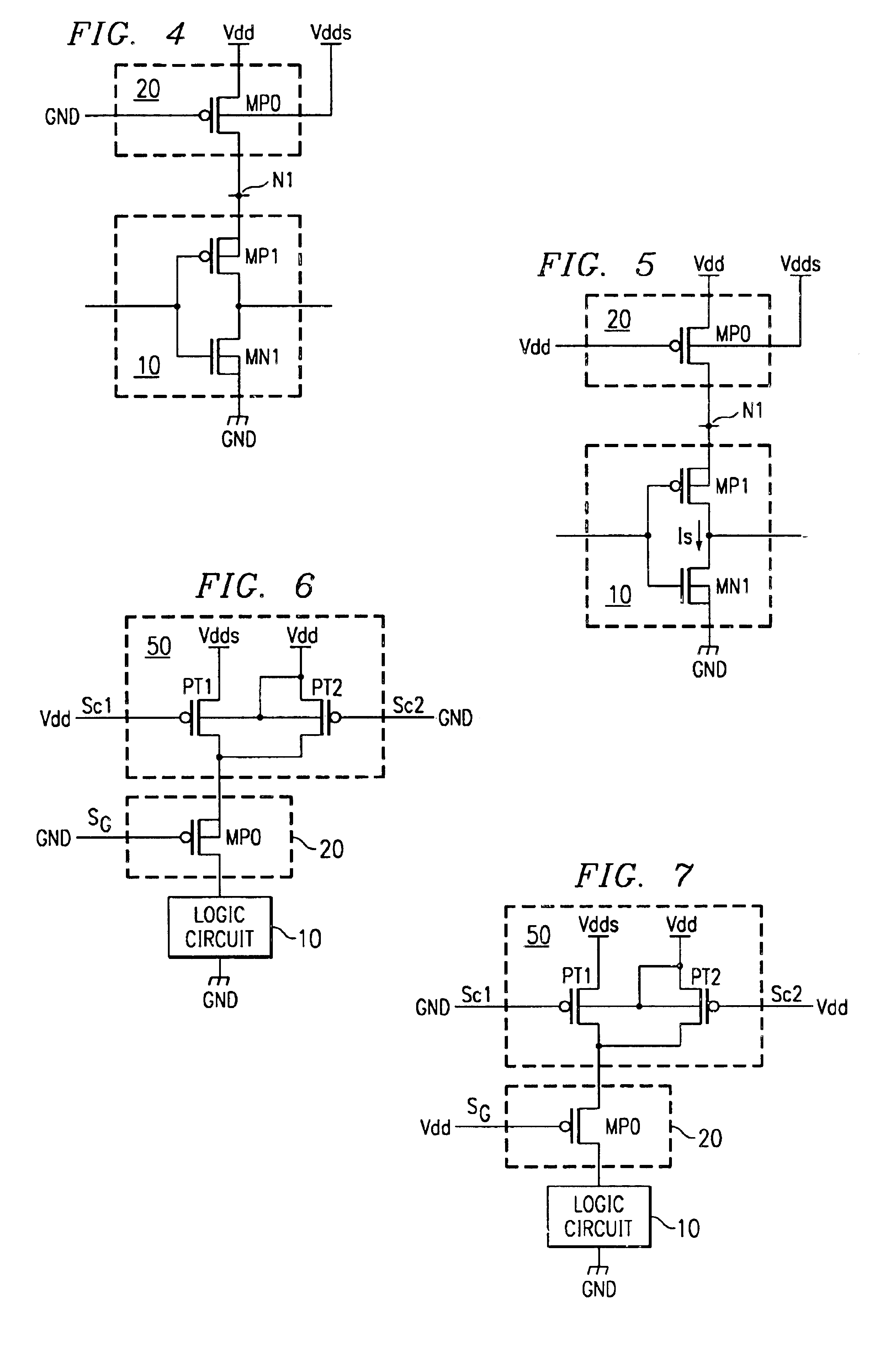
FIG. 6 is a circuit diagram showing a second embodiment of the semiconductor integrated circuit pertaining to the present invention.

As shown in the figure, the semiconductor integrated circuit of the present embodiment is configured with source voltage switching circuit 50 provided in place of the voltage regulator. Source voltage switching circuit 50 switches the level of the source voltage supplied to switching circuit 20 during operation and during standby.

In the aforementioned first embodiment of the semiconductor integrated circuit, the source voltage supplied to switching circuit 20 is switched using voltage regulator 40. The source voltage level needs to be switched quickly according to the operating condition of the semiconductor integrated circuit. For example, when switched from the standby status to the operating status, responsiveness of logic circuit 10 is affected unless the source voltage to be supplied to switching circuit 20 is switched from Vdds to Vdd within sever...

third embodiment

FIG. 8 is a circuit diagram showing a third embodiment of a semiconductor integrated circuit pertaining to the present invention.

As shown in the figure, in the semiconductor integrated circuit of the present embodiment, bulk bias switching circuit 60 is provided; wherein, bulk bias voltage VB is switched and applied to the channel region of pMOS transistor MP0 constituting switching circuit 20.

Logic circuit 10 is a functional circuit for performing a logic operation. Furthermore, although an example of logic circuit 10 configured with a 2-stage MOS inverter is shown in FIG. 8 for the sake of convenience, logic circuit 10 is not limited to said [example].

Switching circuit 20 is configured with pMOS transistor MP0. The source of transistor MP0 is connected to source voltage Vdd supply terminal, and its drain is connected to node N1. Furthermore, node N1 is a virtual source voltage supply terminal of logic circuit 10. Control signal SG is applied to the gate of transistor MP0. Control ...


PUM


Abstract

A semiconductor integrated circuit wherein the circuit area can be minimized, and defects can be detected reliably during a standby status while maintaining the reliability of a gate oxide film. Switching circuit 20 is provided between logic circuit 10 and source voltage Vdd supply terminal. While in an operating status, 0 V voltage is applied to the gate of transistor MP0 of switching circuit 20, and bias voltage VB equal to or slightly lower than source voltage Vdd is applied to its channel region in order to reduce the threshold voltage of transistor MP0 and increase its current driving capability. While in a standby status, a voltage equal to source voltage Vdd is applied to the gate of transistor MP0, a voltage lower than the source voltage is applied to the source, and bulk bias voltage VB equal to or higher than source voltage Vdd is applied to the channel region in order to minimize the drain current of transistor MP0, so that current path of logic circuit 10 is cut off, and the occurrence of leakage current is suppressed.

Description

FIELD OF THE INVENTIONThe present invention pertains to a semiconductor integrated circuit, for example, a semiconductor integrated circuit by which power consumption can be reduced by suppressing leakage current.BACKGROUND OF THE INVENTIONIn recent years, as semiconductor integrated circuit technology has progressed, mobile communication terminals, compact solid-state audio players, and portable semiconductor devices, such as laptop personal computers, have become pervasive. Since a necessary power is supplied to these semiconductor devices, it is absolutely essential to reduce the power consumption in order to allow them to operate for a long time.In the case of a semiconductor integrated circuit, voltage reduction is one effective method for achieving low power consumption. Thus, semiconductor integrated circuits having a source voltage of 1.0 V or lower have been prototyped and have already been brought to the commercial stage. When the source voltage drops and becomes close to ...

Claims


Application Information

Patent Timeline
IPC IPC(8): H01L21/70H01L21/822H01L31/0264H01L31/0336H01L27/04H03K19/0948H03K17/687H03K19/003G11C5/14H03K19/00
CPCG11C5/14H03K19/00315H03K19/0016
Inventor TAKAHASHI, HIROSHITAKEGAMA, AKIHIROTOYONOH, YUTAKAAWAKA, KAORUTANAKA, TSUYOSHIIKENO, RIMON
Owner TEXAS INSTR INC
Why Eureka
Try Eureka