Charge pump level converter (CPLC) for dual voltage system in very low power application

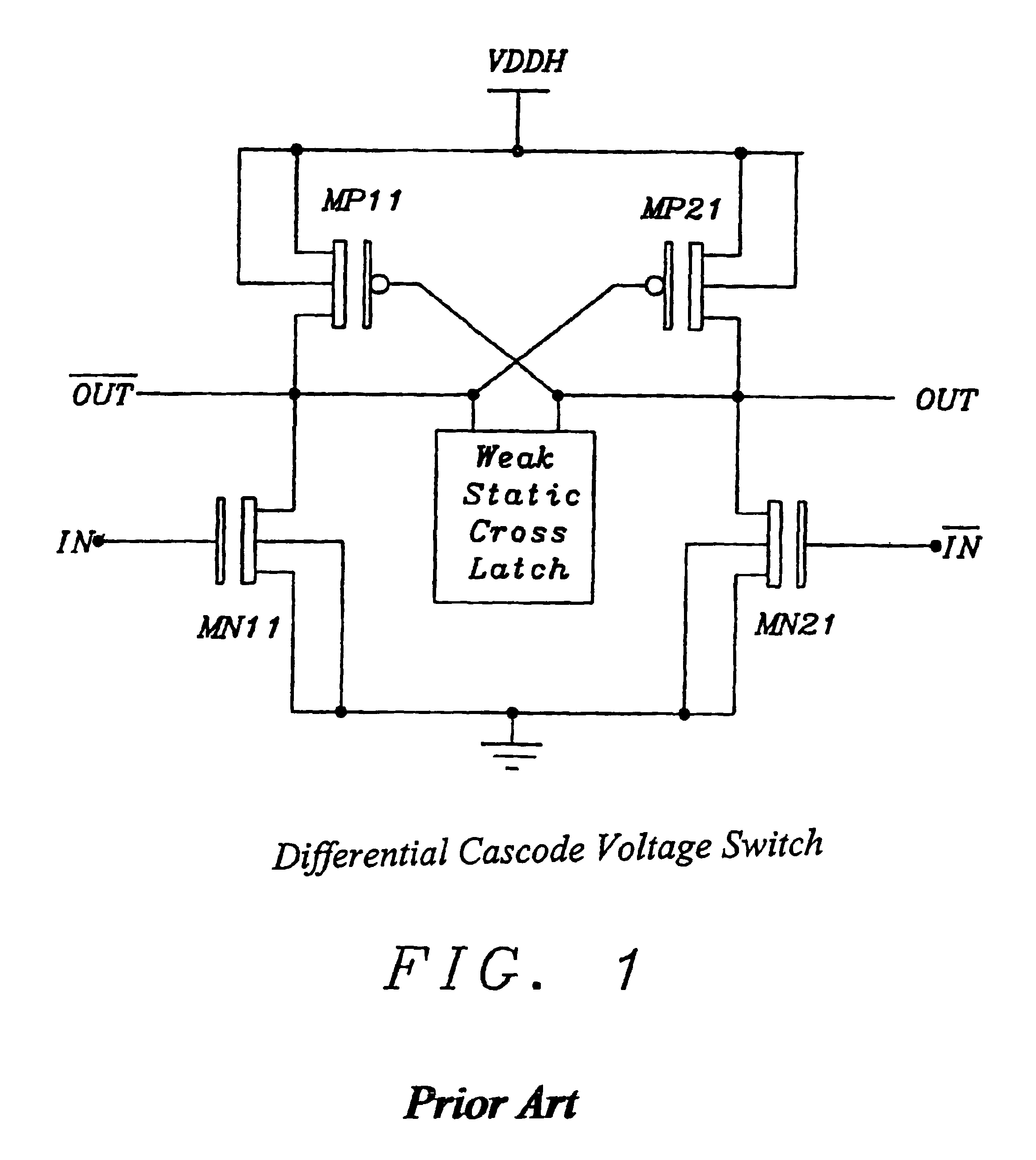
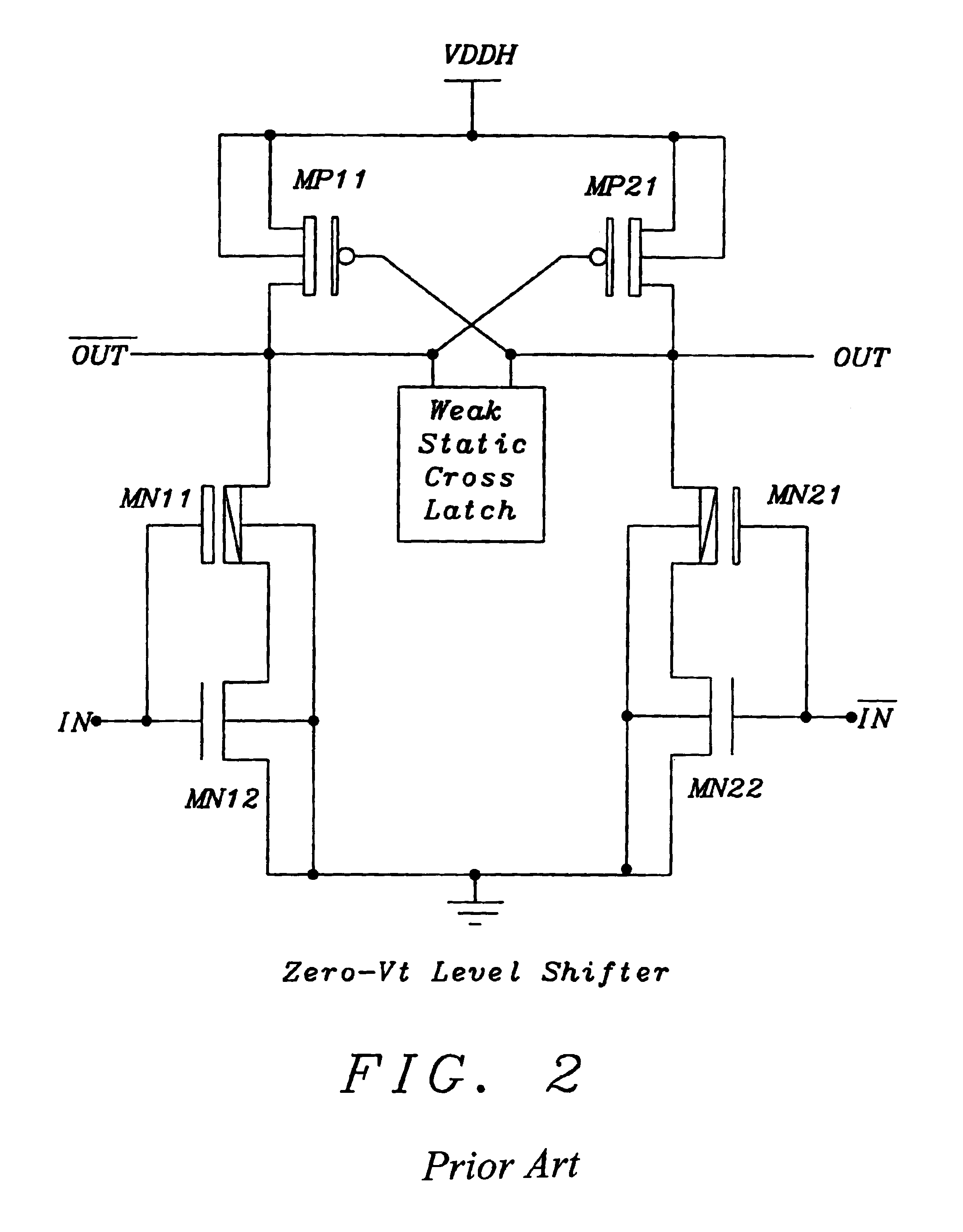
a converter and level technology, applied in logic circuits, pulse automatic control, pulse technique, etc., can solve the problems of small layout area, failure of dcvs shown in fig. 1, and failure of all above related ar

Inactive Publication Date: 2005-03-08
TAIWAN SEMICON MFG CO LTD
View PDF10 Cites 63 Cited by
  • Summary
  • Abstract
  • Description
  • Claims
  • Application Information

AI Technical Summary

Problems solved by technology

The DCVS shown in FIG. 1 becomes too slow or fails, and is unacceptable because the core voltage approaches or is even lower than the threshold voltage Vt of the thick oxide device of the 3.3-V MOSFET.
This approach is utilizing a large layout area, it is too slow due to the large zero-Vt NMOS device which has large parasitic capacitive loading on the output node, and the fabrication process must provide for native device which is not readily available in conventional CMOS fabrication process.
However none of the above related art achieve high speed from 1-V to 3.3-V I / O interface, use only basic CMOS devices and result in smaller layout area.

Method used


Image

  • Charge pump level converter (CPLC) for dual voltage system in very low power application
  • Charge pump level converter (CPLC) for dual voltage system in very low power application
  • Charge pump level converter (CPLC) for dual voltage system in very low power application

Examples


Embodiment Construction

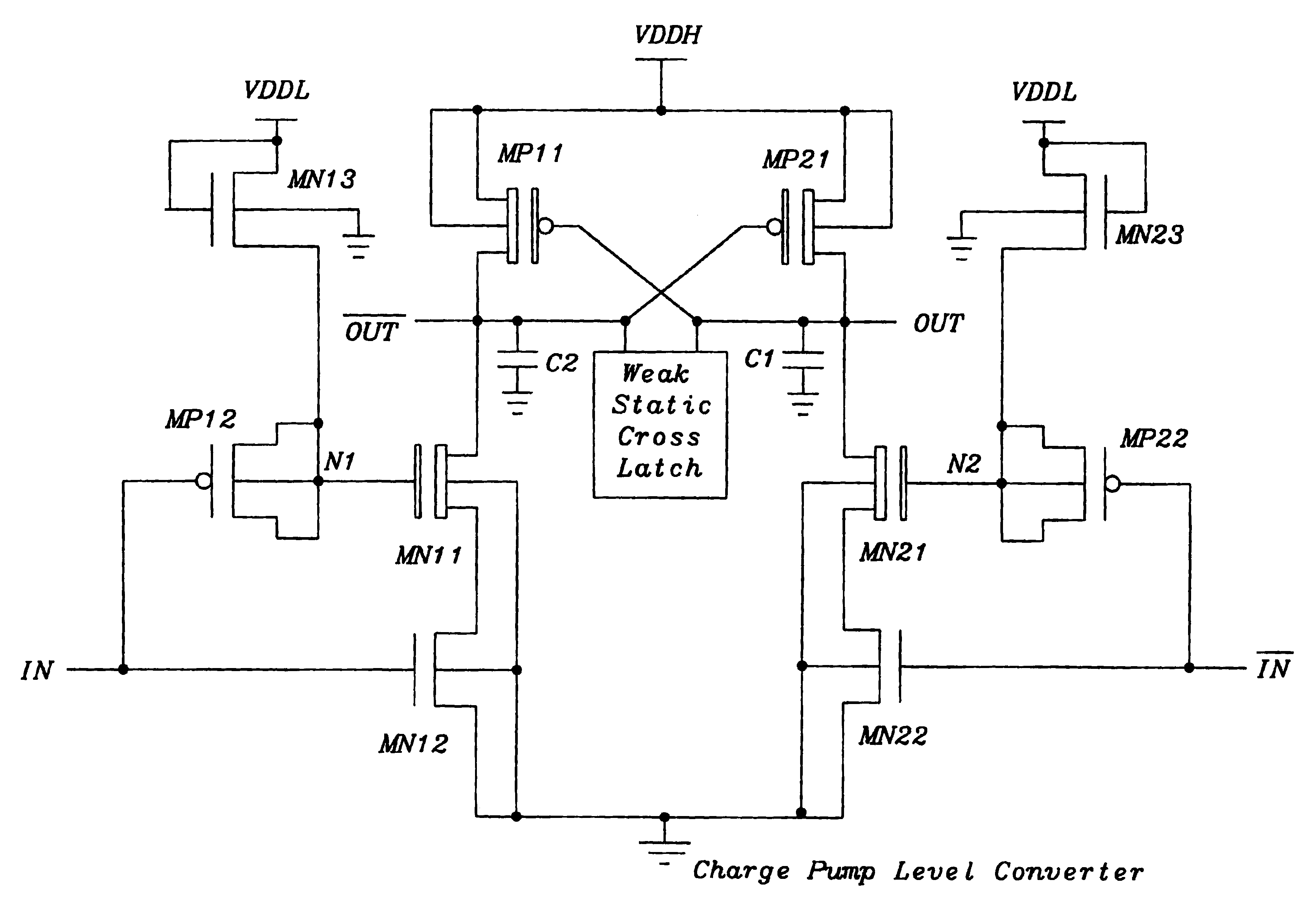
FIG. 3 shows the topology for the level shift charge pump level converter (CPLC) according to the present invention.

The CPLC is comprised of two inputs and two outputs.

IN is the inphase or true input, and {overscore (IN)} is the out-of-phase or complement input. The outputs are: OUT which is the inphase or true output, and {overscore (OUT)} which is the out-of-phase or complement output. The circuit operates between ground and VDDH, which is the higher I / O voltage, and ground and VDDL which is the lower core voltage supply.

The operation of the circuit is as follows:with the in-phase input IN at logical “0” (ground) and the out-of-phase input {overscore (IN)} at logical “1” (VDDL), node N1 is pre-charged to (VDDL-Vtn) through the diode connected NMOS device MN13; when the out-of phase input {overscore (IN)} is at logical “0” and the in-phase input IN is at logical “1”, node N2 is pre-charged to (VDDL-Vtn) through the diode connected NMOS device MN23.

Vtn is the threshold of NMOS devic...


PUM


Abstract

Recent efforts are underway to develop LSI circuits that operate at power supply voltages of 1-V or lower. It is a desire that this low core voltage circuits interface to 3.3-V I/O supply. A charge pump level converter for dual power supply application is proposed using low power and high speed interface to higher I/O supply. This circuit does not consume DC power it is suitable for low power and high speed interface and can be implemented using complementary metal-oxide-semiconductor (CMOS) fabrication processes.

Description

BACKGROUND OF THE INVENTION1. Field of the InventionThe present invention relates to CMOS (complementary metal-oxide semiconductor) Integrated circuits (IC's) and more specifically to a charge pump level converter (CPLC) for translating low core 1-V to high-speed 3.3-V I / O interface.2. Description of Related ArtAdvances in CMOS technology are driving the operating core voltage of IC's lower. As device dimensions shrink, the voltage of the core logic, scales down proportionally in order to avoid gate-oxide breakdown and hot electron effects.However, the 3.3-V I / O interface remains constant.Complex integrated circuits operating with supply voltages of 1-V or lower have been demonstrated. In order to incorporate these circuits into existing systems it is necessary to provide interfaces from the low voltage logic to logic devices operating at 3.3-V or higher.The often seen level converter is DCVS (Differential Cascode Voltage Switch) shown in FIG. 1. The DCVS shown in FIG. 1 becomes too...

Claims


Application Information

Patent Timeline
Patent Type & Authority Patents(United States)
IPC IPC(8): H03K3/356H03K3/00
CPCH03K3/356113
Inventor YU, TSUNG-HSIN
Owner TAIWAN SEMICON MFG CO LTD
Why Eureka
Try Eureka