Semiconductor memory device with memory cells arranged in high density

a memory cell and high density technology, applied in semiconductor devices, digital storage, instruments, etc., can solve the problems of inability to accurately perform sensing operations, storage data may be lost, and difficulty in accurate sensing operations, so as to reduce the active region of memory cells in the vertical and horizontal directions, reduce the layout area size of twin cells, and reduce the unit area of memory cells.

Inactive Publication Date: 2005-03-15
RENESAS TECH CORP
View PDF10 Cites 23 Cited by
  • Summary
  • Abstract
  • Description
  • Claims
  • Application Information

AI Technical Summary

Benefits of technology

An object of the present invention is to provide a semiconductor memory device allowing high-density arrangement of memory cells.
By arranging the memory cell active region such that it crosses the word and bit lines at an angle different from the right angle, the memory cell active region can correspond to a hypotenuse region of a right triangle. Therefore, in comparison with the arrangement in which the active region crosses the word line at the right angle, the lengths of the memory cell active region in the vertical and horizontal directions can be reduced. As a result, a unit area of the memory cell can be decreased, and the layout area size of twin cells can be reduced.

Problems solved by technology

As a result, a sensing operation cannot accurately be performed.
As a result, it becomes difficult to perform an accurate sensing operation.
Thus, storage data may be lost through a leakage current.
The shorter refresh intervals reduce the system processing efficiency, because the DRAM is generally inaccessible during the refresh operation.
In addition, power dissipation for the refresh operation is increased.
Thus, a twin cell mode DRAM with a large storage capacity cannot easily be realized.
As a result, a regularity of a layout pattern is impaired.
As a result, a problem arises that more current is consumed upon selection of word lines.

Method used


Image

  • Semiconductor memory device with memory cells arranged in high density
  • Semiconductor memory device with memory cells arranged in high density
  • Semiconductor memory device with memory cells arranged in high density

Examples


first embodiment

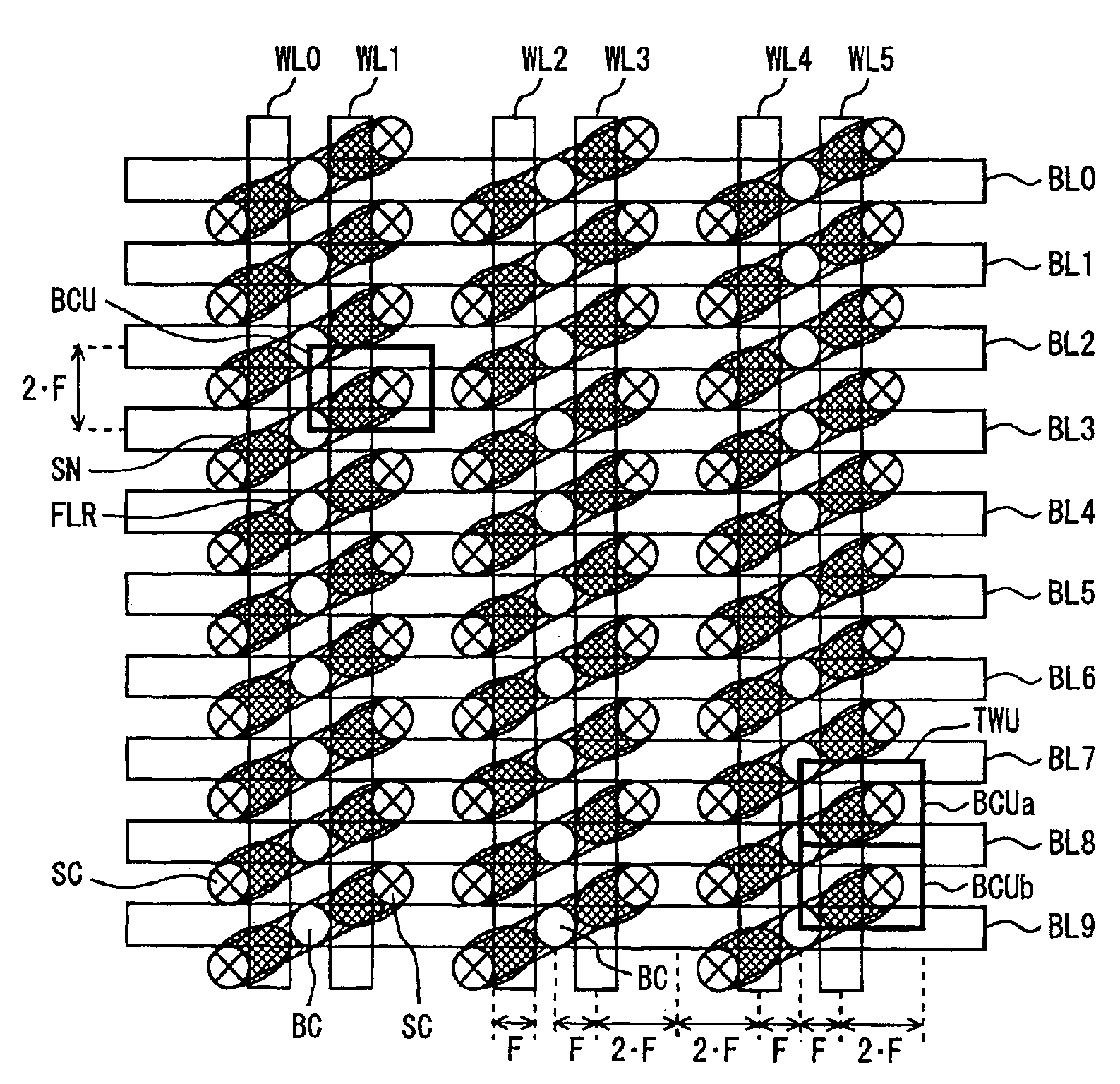
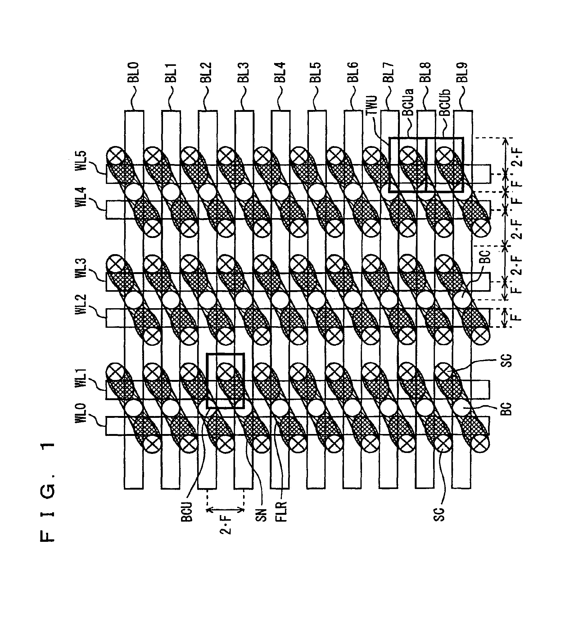
FIG. 1 schematically shows a layout of a memory cell array portion in a semiconductor memory device in accordance with a first embodiment of the present invention. In FIG. 1, word lines WL0 to WL5 are arranged extending in a row direction, while bit lines BL0 to BL9 are arranged extending in a column direction. These word lines WL0 to WL5 and bit lines BL0 to BL9 are arranged crossing with each other in FIG. 1. Each of word lines WL0 to WL5 is made of, for example, a polysilicon interconnection line, while each of bit lines BL0 to BL9 is made of, for instance, a first metal interconnection line at an upper layer.

In a direction crossing word lines WL0 to WL5 and bit lines BL0 to BL9, an active region (a field region) FLR is provided. Two DRAM cells are formed in a single field region FLR.

A bit line contact BC is formed in a crossing portion of field region FLR and bit line BL (generically indicating BL0 to BL9).

In field region FLR, storage node contacts SCs are provided at ends oppos...

second embodiment

FIG. 5 schematically shows a layout of a memory array in a semiconductor memory device in accordance with a second embodiment of the present invention. The layout shown in FIG. 5 is different from the layout in FIG. 1 in the following point. Specifically, a dummy word line DWL (DWL0 to DWL3) is provided in a region between storage node contacts SCs formed in field regions adjacent in a column direction. In other words, dummy word line DWL is provided between word lines WLs arranged at a pitch of 4·F. The other portions of the layout shown in FIG. 5 are similar to those of the layout in FIG. 1. Thus, the same reference numerals are assigned to corresponding portions, and a detailed description thereof will not be repeated.

Dummy word line DWL is formed at the same interconnection line layer as word line WL, and is fabricated through the same manufacturing process as word line WL. Therefore, an additional process and mask are not required for the provision of dummy word line DWL.

A pitc...

third embodiment

FIG. 8 schematically shows a layout of a memory array portion in a semiconductor memory device in accordance with a third embodiment of the present invention. In the layout shown in FIG. 8, a field region FLRA is formed in a region below each of dummy word lines DWL0 to DWL3, and field regions FLRs are formed continuously. Thus, field regions FLRs of memory cells in adjacent rows and adjacent columns are formed continuously, and field regions FLRs are formed extending along one direction. Field region FLRA formed in a region below dummy word line DWL (DWL0 to DWL3) extends linearly in the column direction, and physically connect the field regions provided for opposite storage nodes with respect to the dummy word line.

A ground voltage or a negative voltage Vdm is applied to each of dummy word lines DWL0 to DWL3.

The other configurations in the layout shown in FIG. 8 are similar to those in the layout shown in FIG. 5. Thus, the same reference numerals are assigned to corresponding port...


PUM


Abstract

A field region forming a transistor is provided in a direction crossing a word line and a bit line. A bit line contact is provided corresponding to each bit line in a row direction. Storage node contacts are provided in alignment corresponding to respective columns in the row direction. The size of a basic cell region for forming a single memory cell can be set to 2·F·3·F. Here, F represents a minimum design size. Accordingly, memory cells in a twin cell mode DRAM storing one bit of data with two memory cells can be reduced in size.

Description

BACKGROUND OF THE INVENTION1. Field of the InventionThe present invention generally relates to a semiconductor memory device, and in particular, to a twin cell DRAM (Dynamic Random Access Memory) storing data of one bit with two memory cells. More specifically, the present invention relates to a layout of memory cells in a twin cell mode DRAM.2. Description of the Background ArtIn a DRAM, a memory cell is generally configured of one selection (access) transistor and one capacitor, and data is stored in the capacitor in the form of charges. An electrode node storing the data of the memory cell capacitor is referred to as a storage node. Charges corresponding to data are accumulated at the storage node. An electrode facing this storage node is referred to as a cell plate electrode and receives a voltage of a prescribed level.In data reading, the charges accumulated in the capacitor is transferred to a bit line via the selection transistor of the memory cell. A voltage of the bit line ...

Claims


Application Information

Patent Timeline
Patent Type & Authority Patents(United States)
IPC IPC(8): G11C11/404G11C11/4097G11C11/409G11C11/403H01L27/108G11C11/401H01L21/3205H01L21/8242H01L27/02
CPCG11C11/404G11C11/4097H01L27/10891H01L27/10882H01L27/10885H01L27/0207H10B12/48H10B12/482H10B12/488H01L21/3205
Inventor TSUKIKAWA, YASUHIKO
Owner RENESAS TECH CORP
Why Eureka
Try Eureka