
Constant impedance in CMOS input and output gain stages for a wireless transceiver

a wireless transceiver and gain stage technology, applied in the direction of gain control, multiple-port active network, transmission, etc., can solve the problems of variable amount of reflective power within the circuit, and achieve the effect of reducing potential, simple construction, and efficient operation

Inactive Publication Date: 2005-03-15
MEDIATEK INC
View PDF7 Cites 15 Cited by
  • Summary
  • Abstract
  • Description
  • Claims
  • Application Information

AI Technical Summary

Benefits of technology

It is of further object of the present invention to provide input and output circuits of the type described which are simple in construction and efficient in operation.
Briefly stated, in accordance with the present invention, there is provided a constant resistance path is provided between the input and output of the constant impedance stage. The constant resistance preferably comprises first and second resistors of equal value. The source-drain circuit of a first CMOS transistor is connected across the resistive path. The source-drain circuit of a second CMOS transistor is connected between the junction of the first and second resistors and ground. The gate potential of the first CMOS transistor is controlled by a first digital to analog converter circuit, and the gate potential at the second CMOS transistor is controlled by the output of a second digital to analog converter. Gain, in the present case less than unity gain, is controlled by the level of conductivity of the source draining circuit of the second transistor. The harder the second transistor turns on, the lower the potential at the junction of the first and second resistors. This decrease in the resistance produces a decrease in circuit impedance which requires compensation. At the same time, the output voltage of the first digital to analog converter will decrease. Consequently, the source drain gate of the first transistor conducts less strongly and has a higher effective resistance. This higher effective resistance counteracts the impedance change caused by conduction by the second transmitter in response to a strong RF signal.

Problems solved by technology

Variations in impedance can contribute to degraded signal to noise ratio and will cause various amounts of reflective power within the circuit.

Method used


Image

  • Constant impedance in CMOS input and output gain stages for a wireless transceiver
  • Constant impedance in CMOS input and output gain stages for a wireless transceiver
  • Constant impedance in CMOS input and output gain stages for a wireless transceiver

Examples


Embodiment Construction

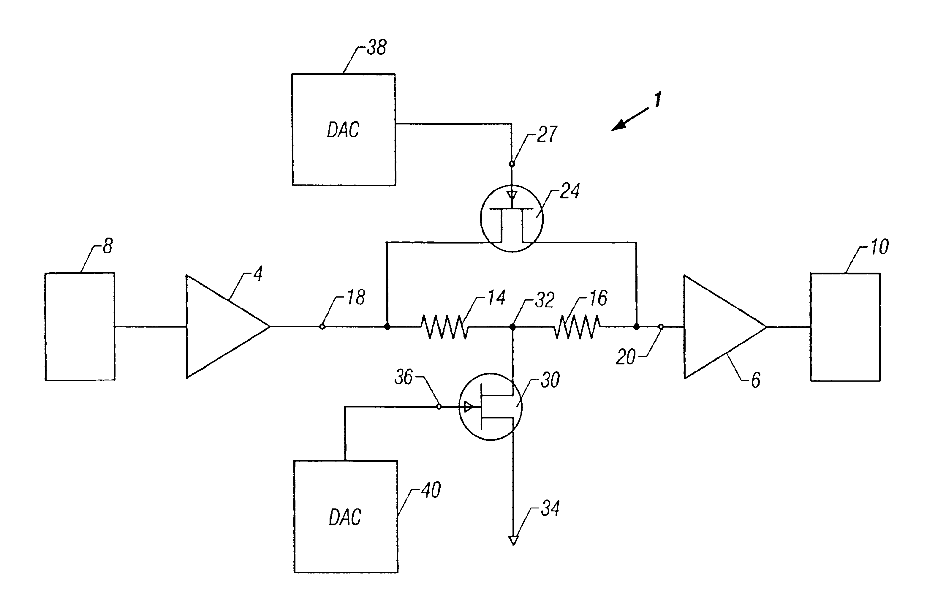
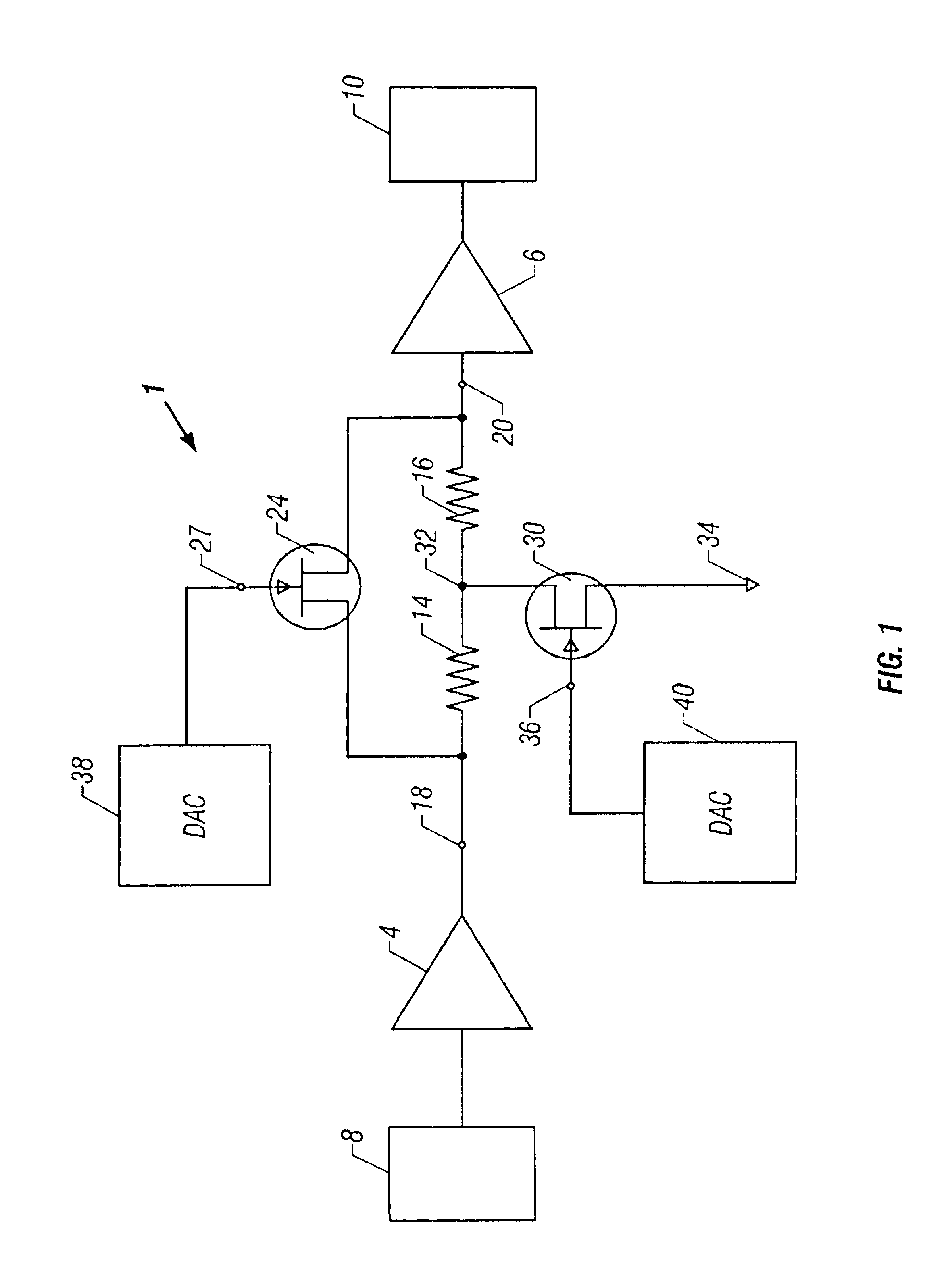
FIG. 1 is an illustration of a constant impedance gain control circuit 1 interacting in the environment of a communications circuit. For brevity, the constant impedance gain control circuit 1 will be called the gain control circuit 1. In the present example, gain will be a factor of less than unity. Thus the gain control circuit 1 could also be referred to as an attenuator. However, at certain levels of description, the labels applied to gain control circuits, attenuators, and filters can effectively be arbitrary. The gain control circuit 1 is connected between amplifiers 4 and 6 in a communications circuit. However, the input means 9 provides the signal which will be operated upon. FIG. 1 is thus illustrative of a transmitter or receiver. In particular illustration in FIG. 1, the transmitter option is illustrated by showing within the input means 9 a Gilbert cell modulator 7 which converts a signal to be transmitted into in-phase, and quadrature grid radio frequency signal. The rad...


PUM


Abstract

An apparatus to provide a stage in a transmitter or receiver operating in wireless frequency ranges performing a gain control function between a final or an initial stage respectively and process circuitry for adjusting gain and providing a constant input impedance at its input and a constant output impedance at its output, providing a direct conversion transceiver in which constant impedance gain control circuits are provided in the receive and transmit paths, all of which are simple in construction and efficient in operation.

Description

FIELD OF INVENTIONThe present invention relates to input or output stages adjacent to an antenna or filter providing constant input and output impedances.BACKGROUND OF THE INVENTIONThe present invention is equally applicable to transmitters, receivers, and transceivers. It will find wide application in many environments. One such environment is the cell phone operating in the 900 MHz range but is applicable to all cell phone bands. It is necessary to regulate power transmitted by a cell phone to avoid interference with adjacent channels and comply with standards. One such standard is Mobile Station-Base Station Compatibility Standard for Dual-Mode Wide Band Spread Spectrum Cellular System, EIA / TIA Interim Standard IS-95, Telecommunications Industry Association, Washington, D.C., 1993.Prior art circuits comprising RF signal circuit elements typically use multiple processing stages, including amplification of RF signal before the signal reaches the antenna where it is transmitted. In ...

Claims


Application Information

Patent Timeline
Patent Type & Authority Patents(United States)
IPC IPC(8): H03H11/24H03H11/02
CPCH03H11/245
Inventor GONYA, SR., DENNIS H.
Owner MEDIATEK INC
Learn More