Double throughput analog to digital converter

a digital converter and double-throughput technology, applied in the field of analog to digital conversion, can solve the problems of waste of power, constant consumption of dc bias current, waste of power, etc., and achieve the effects of reducing the gain bandwidth of the amplifier block, improving the efficiency and throughput of an analog, and reducing power consumption

Active Publication Date: 2005-03-22
MICRON TECH INC
View PDF7 Cites 46 Cited by
  • Summary
  • Abstract
  • Description
  • Claims
  • Application Information

AI Technical Summary

Benefits of technology

The present invention is directed to improving the efficiency and throughput of an analog to digital converter. More specifically, the amplifier block for each stage of an analog to digital converter is provided with a switching network for implementing a double sampling and double conversion analog to digital converter stage. Rather than using one phase of a clock cycle for sampling and another for conversion, the both phases of the clock are used for sampling and conversion. By also using two independent processing blocks per stage, the analog to digital c...

Problems solved by technology

Analog ICs often require the use of, and constantly consume, a DC bias current.
However, the processing performed in the amplifier block is analog processing, and as described below, wasteful in power consumption.
One problem associated with the above ...

Method used


Image

  • Double throughput analog to digital converter
  • Double throughput analog to digital converter
  • Double throughput analog to digital converter

Examples


Embodiment Construction

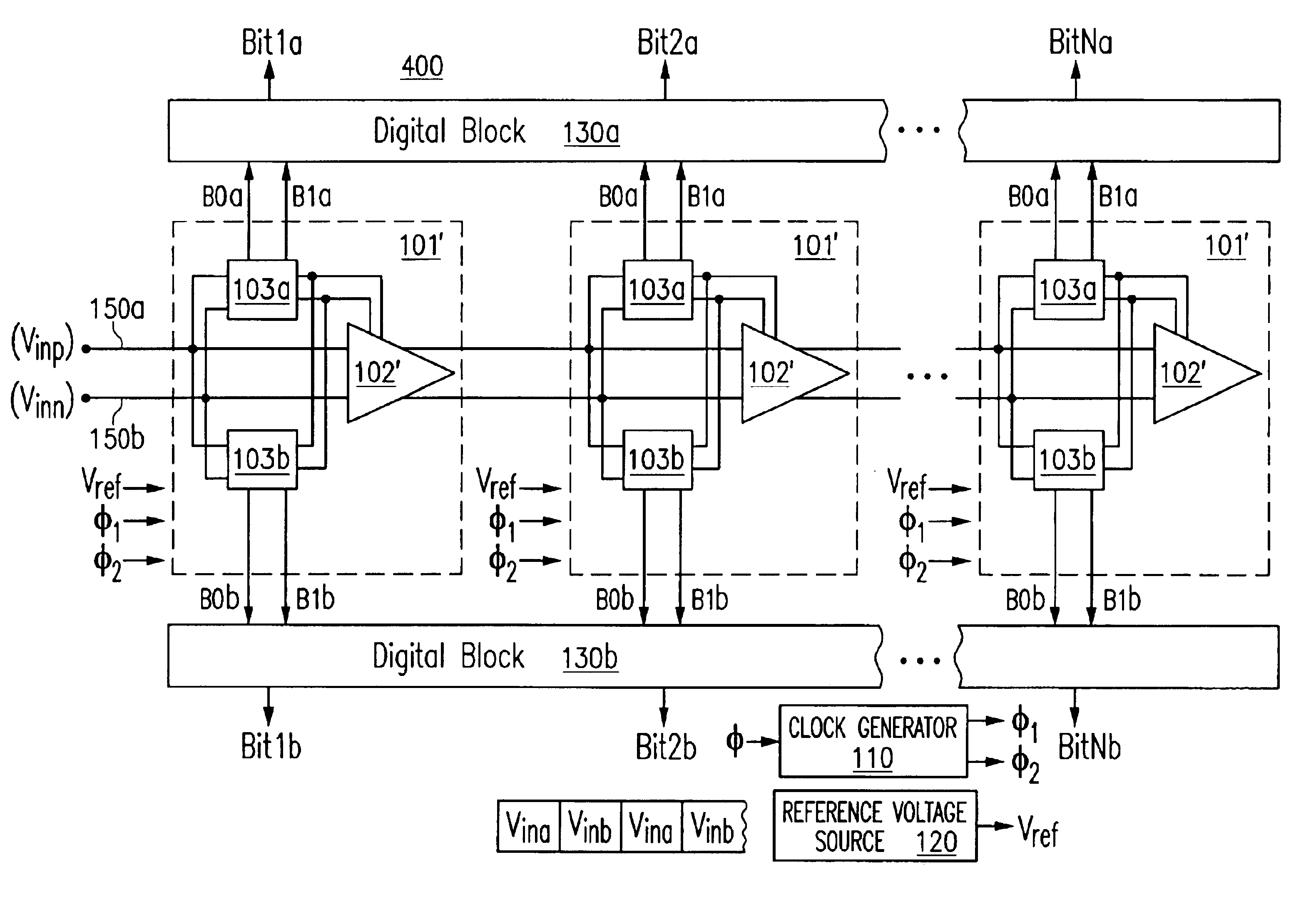
The ADC 400 of the exemplary embodiment shown in FIG. 4 include amplifier blocks 102′ that operate continuously. This is achieved by providing the ADC 400 with two input analog signal streams (Vina, Vinb) to convert into two corresponding digital output signals. As shown in FIG. 4, the two analog input signal streams (Vina, Vinb) are combined in a time multiplexed fashion to form a single input signal, which is presented as a differential signal having components Vinp, Vinn to the input signal pins 150a, 150b. Similarly, the two digital output signals Bit1a, Bit2a, . . . BitNa and Bit1b, Bit2b, . . . , BitNb are output from two digital blocks 130a, 130b as described below.

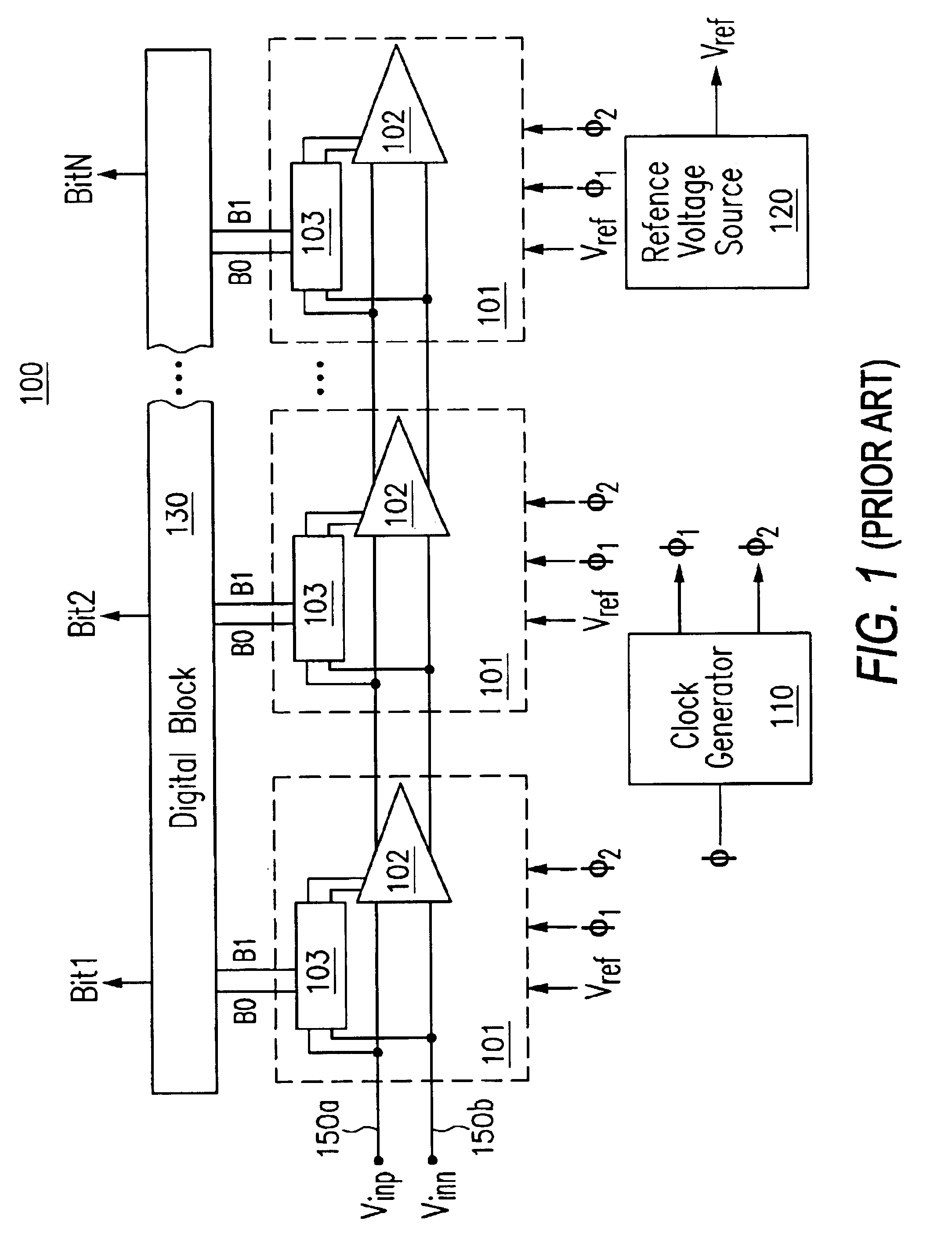
Now referring to the drawings, where like reference numerals designate like elements, FIG. 4 shows a block diagram of the pipelined ADC 400. ADC 400 can include the same clock generator 110 and reference voltage generator 120 as ADC 100 (FIG. 1). Thus, the reference voltage (Vref) and clock signals (φ1, φ2) can ope...


PUM


Abstract

A pipelined analog-to-digital converter features an amplifier block that includes a switching network to implement a double sampling and double conversion principle of operation. The amplifier block utilizes both phases of a clock for sampling and conversion. Additionally, each stage of the analog-to-digital converter is associated with two independent processing blocks. The analog-to-digital converter can achieve double throughput for approximately the same level of power consumption. Alternatively, throughput may be maintained, but the gain-bandwidth of the amplifier block may be reduced by half, thereby halving the DC bias current consumed by the amplifier. Additionally, the output signal of the amplifier itself is not reset to a common mode voltage.

Description

FIELD OF INVENTIONThe present invention relates generally to analog to digital conversion, and more particularly, to a double throughput analog to digital converter.BACKGROUND OF THE INVENTIONAnalog integrated circuits (ICs) are integrated circuits that process analog signals. Examples of such circuits include, for example, amplifiers, reference current sources, and reference voltage sources. Analog ICs often require the use of, and constantly consume, a DC bias current. Digital integrated circuits are ICs which process digital signals. Examples of digital integrated circuits include, for example, logical circuit and state machines, such as processors. Digital circuits with complementary metal oxide semiconductor (CMOS) logic generally do not use a DC bias current.Some integrated circuits, however, process both analog and digital signals. Such circuits are known as mixed signal integrated circuits. Mixed signal ICs generally require the use of a DC bias current supply. A common exam...

Claims


Application Information

Patent Timeline
IPC IPC(8): H03M1/12H03M1/00H03M1/06H03M1/38H03M1/44
CPCH03M1/1245H03M1/002H03M1/442H03M1/0695
Inventor ZADEH, ALI E.ANG, LIN P.
Owner MICRON TECH INC
Why Eureka
Try Eureka