Micromirrors with mechanisms for enhancing coupling of the micromirrors with electrostatic fields

a micromirror and electrostatic field technology, applied in the field of microelectromechanical systems, can solve the problems of short cathode lifetime, low light efficiency of devices, and use of bulky and expensive vacuum tubes

Inactive Publication Date: 2005-03-29
VENTURE LENDING & LEASING IV +1
View PDF6 Cites 48 Cited by
  • Summary
  • Abstract
  • Description
  • Claims
  • Application Information

AI Technical Summary

Benefits of technology

In another embodiment of the invention, a micromirror array device is disclosed. The micromirror array device comprises: a substrate; a reflective mirror plate connected to the substrate via a hinge and a hing

Problems solved by technology

A disadvantage of the Eidophor system is that the oil film is polymerized by constant electron bombardment and oil vapors result in a short cathode lifetime.
A disadvantage of both of these systems is their use of bulky and expensive vacuum tubes.
Although the switching voltage of this SLM is lowered by connecting the deflectable mirror elements at only one corner, the device has low light efficiency due to the small fractional active area.
In addition, diffraction from the addressing circuitry lowers the contrast ratio (modulation depth) of the display.
If this distance is one-quarter of a wavelength, light directly reflected from the two surfaces will interfere destructively and the device will act as a diffraction grating, sending light into diffracted orders.
When the ribbons a

Method used


Image

  • Micromirrors with mechanisms for enhancing coupling of the micromirrors with electrostatic fields
  • Micromirrors with mechanisms for enhancing coupling of the micromirrors with electrostatic fields
  • Micromirrors with mechanisms for enhancing coupling of the micromirrors with electrostatic fields

Examples


Embodiment Construction

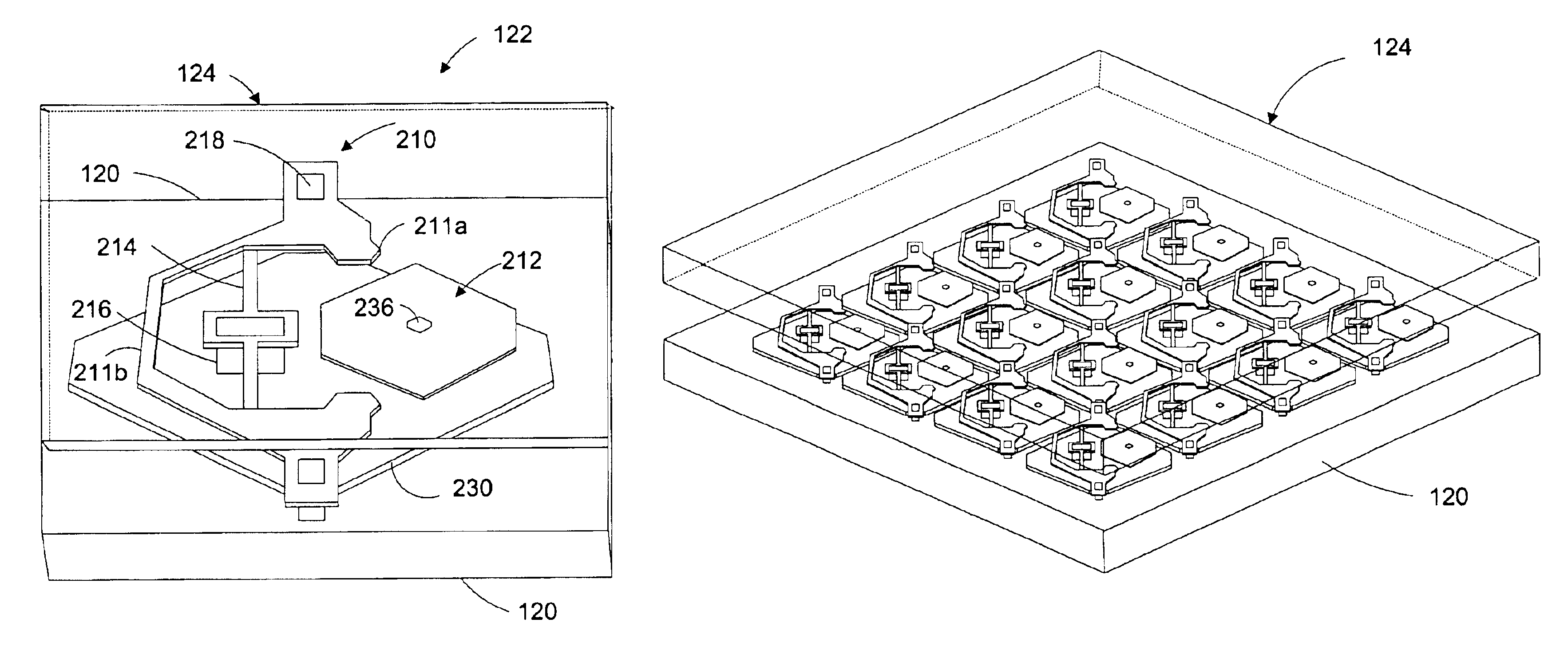
Processes for micro-fabricating a MEMS device such as a movable micromirror and micromirror array are disclosed in U.S. Pat. Nos. 5,835,256 and 6,046,840 both to Huibers, the subject matter of each being incorporated herein by reference. A similar process for forming MEMS movable elements (e.g. micromirrors) on a wafer substrate (e.g. a light transmissive substrate or a substrate comprising CMOS or other circuitry) is illustrated in the present application. By “light transmissive”, it is meant that the material will be transmissive to light at least in operation of the device (The material could temporarily have a light blocking layer on it to improve the ability to handle the substrate during manufacture, or a partial light blocking layer for decreasing light scatter during use. Regardless, a portion of the substrate, for visible light applications, is preferably transmissive to visible light during use so that light can pass into the device, be reflected by the micromirrors, and p...


PUM


Abstract

A micromirror device is disclosed, along with a method of making such a micromirror device that comprises a mirror plate, a hinge and an extension plate. The extension plate is formed on the mirror plate and between the mirror plate and the electrode associated with the mirror plate for rotating the mirror plate. The extension plate can be metallic or dielectric. Also disclosed is a method of making such a micromirror device. In particular, the extension plate is formed after the formation of the mirror plate. Moreover, also disclosed is a projection system that comprises a spatial light modulator having an array of such micromirrors, as well as a light source, condensing optics, wherein light from the light source is focused onto the array of micromirrors, projection optics for projecting light selectively reflected from the array of micromirrors onto a target, and a controller for selectively actuating the micromirrors in the array.

Description

TECHNICAL FIELD OF THE INVENTIONThe present invention is related generally to the art of microelectromechanical systems, and, more particularly, to micromirrors with mechanisms for enhancing coupling of micromirrors with electrostatic fields.BACKGROUND OF THE INVENTIONSpatial light modulators (SLMs) are transducers that modulate an incident beam of light in a spatial pattern in response to an optical or electrical input. The incident light beam may be modulated in phase, intensity, polarization, or direction. This modulation may be accomplished through the use of a variety of materials exhibiting magneto-optic, electro-optic, or elastic properties. SLMs have many applications, including optical information processing, display systems, and electrostatic printing.An early SLM designed for use in a projection display system is described by Nathanson, U.S. Pat. No. 3,746,911. The individual pixels of the SLM are addressed via a scanning electron beam as in a conventional direct-view cat...

Claims


Application Information

Patent Timeline
IPC IPC(8): G02B26/08G02B26/00H01LH01L21/00
CPCG02B26/0841G02B26/08G02B26/00
Inventor PATEL, SATYADEV R.HUIBERS, ANDREW G.
Owner VENTURE LENDING & LEASING IV
Why Eureka
Try Eureka