Structure and method for index-guided buried heterostructure AlGaInN laser diodes

a laser diode and heterostructure technology, applied in semiconductor lasers, laser details, electrical devices, etc., can solve the problems of relatively weak waveguide and fabrication difficulties, and achieve the effects of improving the far-field radiation pattern, low threshold current, and improving mode stability

Inactive Publication Date: 2005-04-05
XEROX CORP
View PDF11 Cites 36 Cited by
  • Summary
  • Abstract
  • Description
  • Claims
  • Application Information

AI Technical Summary

Benefits of technology

[0007]Both index-guided buried heterostructure AlGalnN laser diodes and self-aligned index guided buried heterostructure AlGalnN laser diodes provide improved mode stability and low threshold current when compared to conventional ridge waveguide structures. A structure for the index-guided buried heterostructure AlGalnN laser diode in accordance with the invention typically uses insulating AlN, AlGaN or p-doped AlGaN:Mg for lateral confinement and has a narrow (typically about 1-5 μm in width) ridge which is the location of the narrow active stripe of the laser diode which is defined atop the ridge. The narrow ridge is surrounded by an epitaxially deposited film having a window on top of the ridge for the p-electrode contact. The ridge is etched completely through the active region of the laser diode structure to the short period superlattice n-cladding layer. Typically, use of a short period superlattice allows doubling of the cladding layer thickness without cracking. This reduces the intensity of the light lost due to leakage by about 2 orders of magnitude with an accompanying improvement in the far-field radiation pattern in comparison with conventional structures. Junction surfaces are exposed by the ridge etch and these junction surfaces contribute surface states which prevent injected carriers from filling conduction or valence band states needed for a population inversion. However, the epitaxial regrowth of a high bandgap material passivates the surface states because the interface between the overgrown material and the ridge structure is perfectly coherent.
[0008]The structure for the self-aligned, index guided, buried heterostructure AlGalnN laser diode uses the p-cladding layer to also function as the burying layer to provide strong lateral optical confinement and strong lateral carrier confinement. The p-cladding layer / burying layer is typically AlGaN:Mg. The structure for the self-aligned, index guided, buried heterostructure laser diode is simpler than for the index-guided, buried heterostructure AlGalnN laser diode. The laser structure is grown through the active quantum well and waveguide region followed by etching a narrow laser ridge down to the n-bulk cladding layer. The p-type cladding / burying layer is then overgrown around the ridge along with the p-contact layer. Subsequent laser processing is simple since the two-step growth process results in a lateral waveguide and carrier confinement structure which does not require the creation of contact windows. Hence, the laser processing required is basically a broad area laser fabrication sequence. Additionally, the comparatively large p-contact area allowed by the self-aligned architecture contributes to a lower diode voltage and less heat during continuous wave operation of the laser diode.

Problems solved by technology

While a ridge waveguide provides for single spatial mode emission in blue lasers, the waveguiding provided is relatively weak.
Additionally, there are fabrication difficulties because the ridge must be etched to extend sufficiently close to the laser active region without the ability to use an etch stop to prevent material damage to the laser active region since chemical etching is not applicable to GaN materials.

Method used


Image

  • Structure and method for index-guided buried heterostructure AlGaInN laser diodes
  • Structure and method for index-guided buried heterostructure AlGaInN laser diodes
  • Structure and method for index-guided buried heterostructure AlGaInN laser diodes

Examples


Embodiment Construction

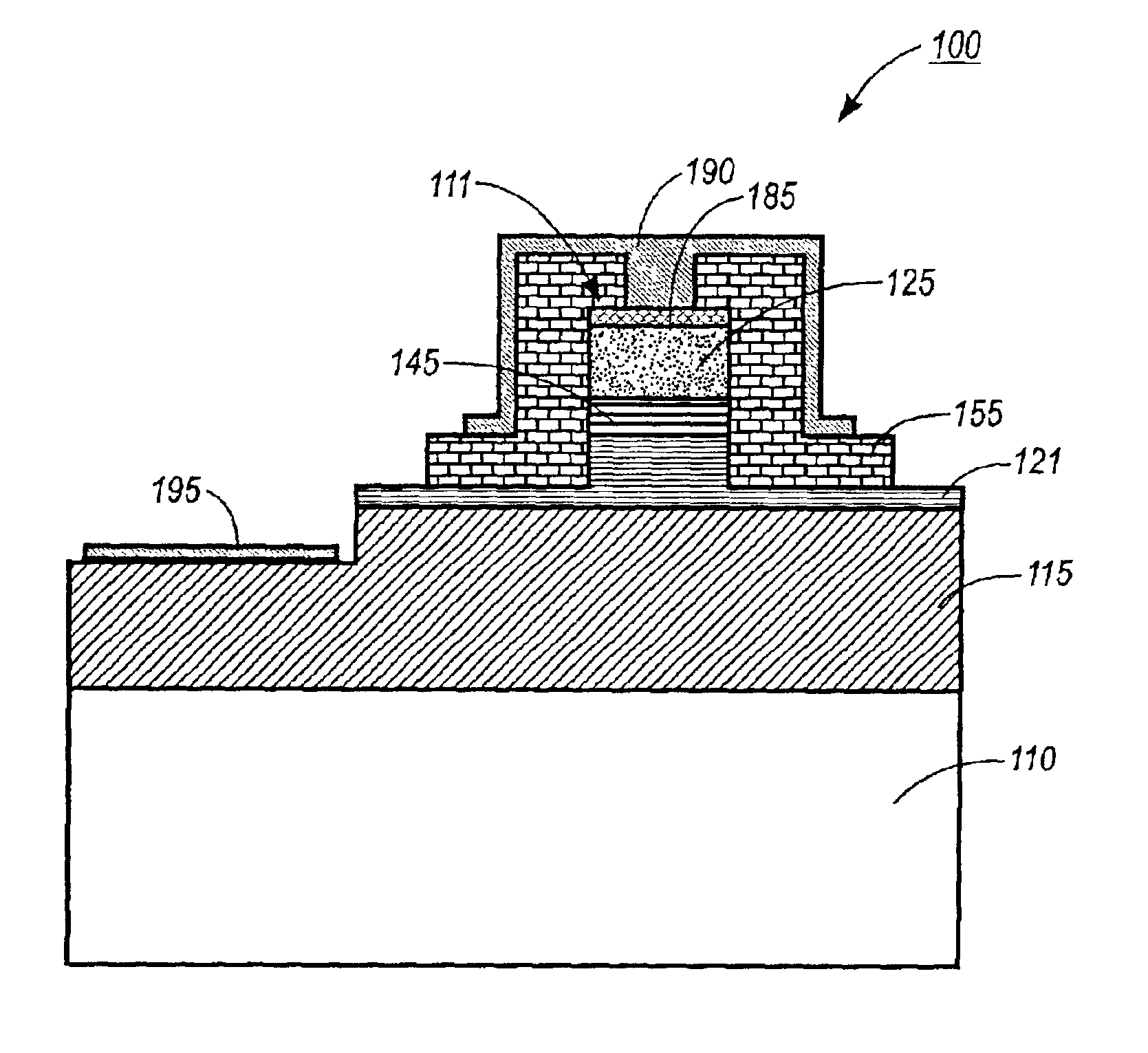
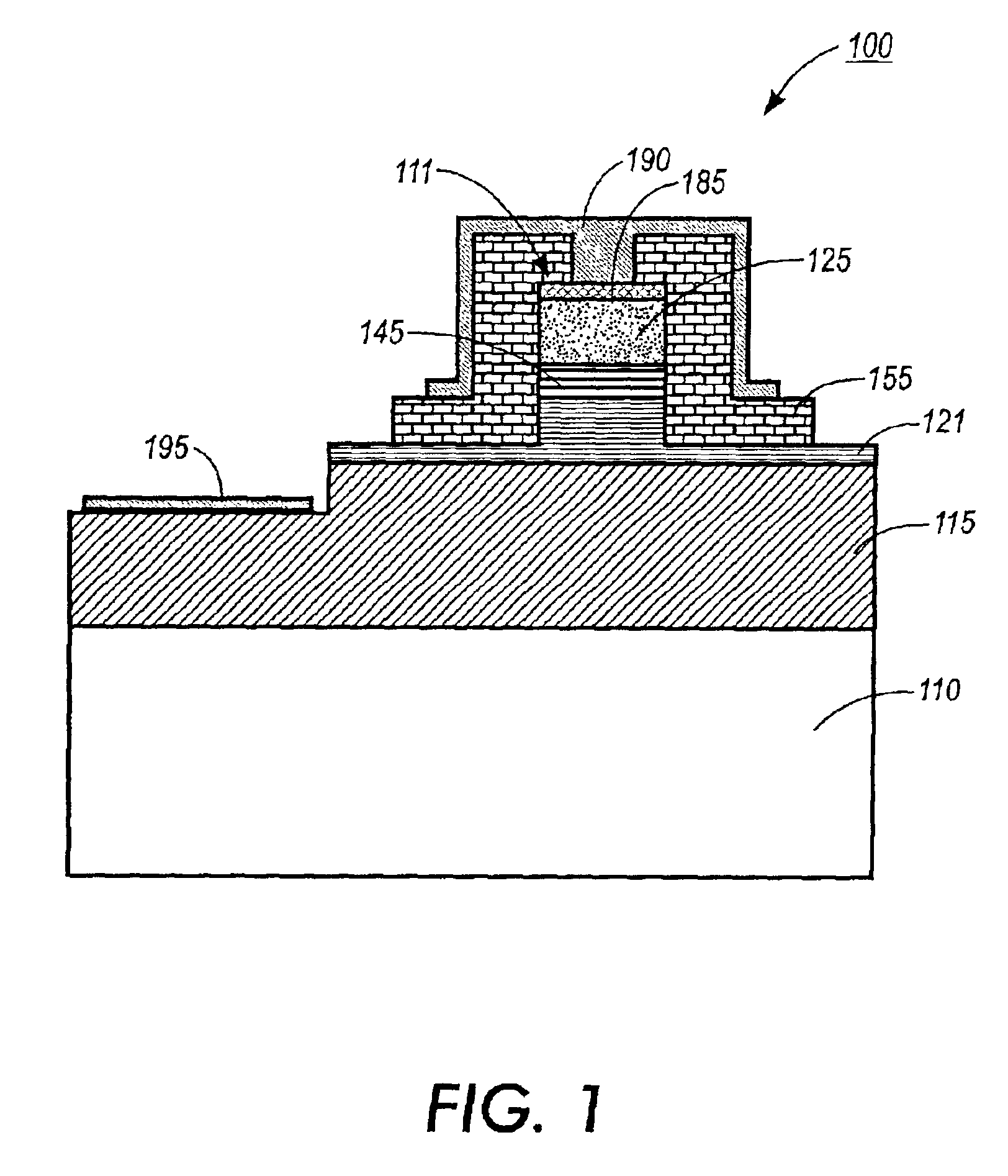
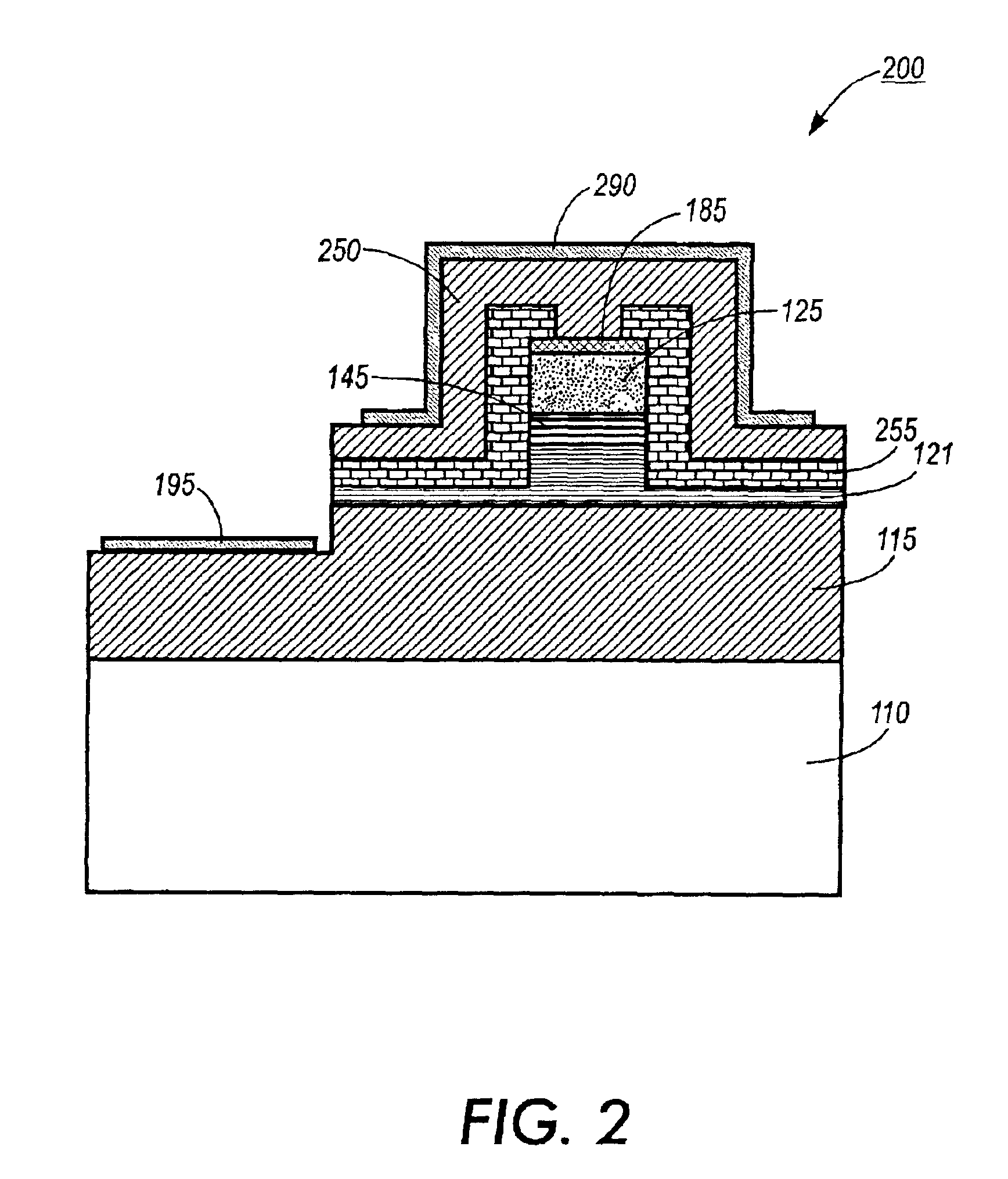
[0016]FIG. 1 shows index-guided, buried heterostructure AlGalnN laser diode structure 100 in accordance with the present invention. GaN:Si layer 115 is positioned on Al2O3 growth substrate 110 and in one embodiment layer 115 may be made of AlGaN:Si to reduce optical leakage. Short period superlattice n-cladding structure 121, typically made up of alternating layers of Al0.15Ga0.85N:Si and GaN:Si each with a typical thickness of about 20 Å, is positioned below the GaN n-waveguide layer (not shown in FIG. 1) at the bottom of InGaN multiple quantum well structure 145. Introduction of short period superlattice n-cladding structure 121 allows increased cladding thickness to significantly reduce leakage of the transverse optical mode and results in an improved transverse far-field pattern for laser diode structure 100. For example, a typical leakage of about 7% may be reduced to 0.5%. The far-field beam pattern approaches a Gaussian far-field beam.

[0017]P-cladding layer 125, typically Al0...


PUM


Abstract

An index-guided buried heterostructure AlGalnN laser diode provides improved mode stability and low threshold current when compared to conventional ridge waveguide structures. A short period superlattice is used to allow adequate cladding layer thickness for confinement without cracking. The intensity of the light lost due to leakage is reduced by about 2 orders of magnitude with an accompanying improvement in the far-field radiation pattern when compared to conventional structures.

Description

CROSS REFERENCE TO RELATED APPLICATIONS[0002]This application is a divisional of application(s) No(s). 09 / 408,458, filed Sep. 29, 1999 now U.S. Pat. No. 6,570,898.[0003]This application is related to commonly assigned, concurrently filed Bour et al. U.S. patent application entitled “STRUCTURE AND METHOD FOR SELF-ALIGNED, INDEX-GUIDED BURIED HETEROSTRUCTURE AlGalnN LASER DIODES” (application Ser. No. 09 / 408,415) which is included by reference in its entirety.FIELD OF INVENTION[0004]This invention relates to nitride based blue laser diodes.BACKGROUND OF INVENTION[0005]Nitride based blue laser diodes are being developed for printing and optical data storage applications. The first AlGalnN laser diodes were broad area lasers providing no control over the laser diode's various spatial modes. Most applications, however, require the laser diode to operate in a single spatial mode. One way of achieving single spatial mode operation for AlGalN blue laser diodes is to use a ridge waveguide st...

Claims


Application Information

Patent Timeline
Patent Type & Authority Patents(United States)
IPC IPC(8): H01S5/323H01S5/00H01S5/20H01S5/227H01S5/343
CPCH01S5/32341H01S5/2004H01S5/2275H01S2304/00H01S2301/18
Inventor BOUR, DAVID P.KNEISSL, MICHAEL A.ROMANO, LINDA T.
Owner XEROX CORP
Why Eureka
Try Eureka