

Aspherical microstructure, and method of fabricating the same
a microstructure and aspherical technology, applied in the field of aspherical microstructure, can solve the problems of difficult to fabricate concave molds with a uniform profile on the surface of the substrate, inability to achieve the desired profile of etching of the substrate, and large area of concave molds, so as to increase the fill-factor and the size of the aspherical microstructure, and the effect of easy control of the aspherical profil
- Summary
- Abstract
- Description
- Claims
- Application Information
AI Technical Summary
Benefits of technology
Problems solved by technology
Method used
Image

Examples
first embodiment
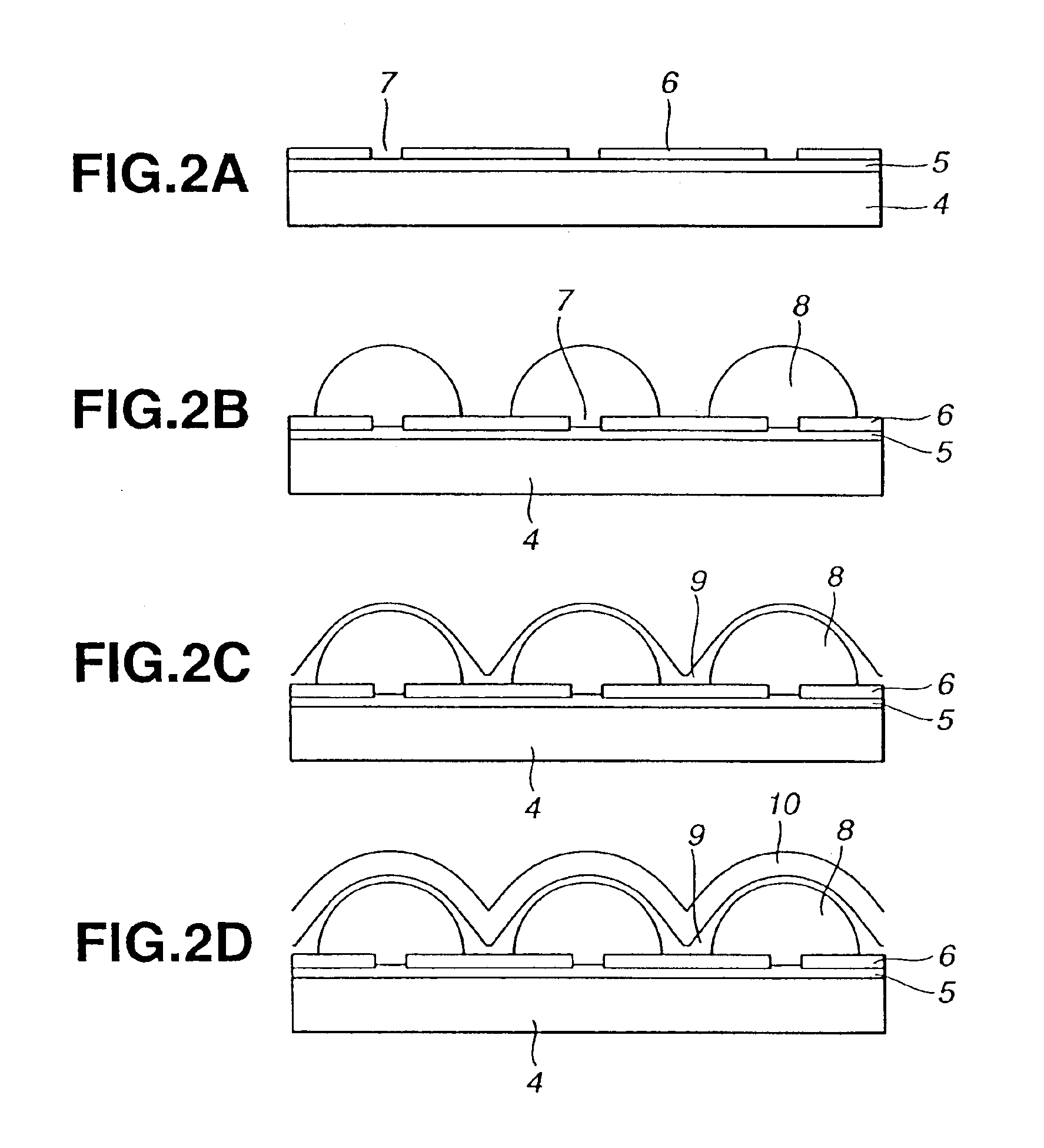
a mold for an aspherical microlens array of the present invention will be described with reference to FIGS. 2A to 2D, which are cross-sectional views in the horizontal direction of adjacent elements arranged in a two-dimensional array. In the first embodiment, a silicon wafer with sides of 1.5 inches×1 inch is used as a substrate 4. The wafer 4 is thermally oxidized using an oxidizing gas, and layers of silicon dioxide with a thickness of 1 μm are formed on opposite surfaces of the wafer 4. Pt is then layered with a thickness of 200 nm on the above wafer 4 using a sputtering method. An electrode layer 5 is thus formed.
A photoresist is then deposited to form an insulating mask layer 6. Further, exposure and development of the photoresist are performed using a photolithography to expose the electrode layer 5 in a predetermined pattern and form a plurality of openings 7 in the photoresist, as illustrated in FIG. 2A. The opening 7 has a circular shape with a diameter of 5 μm. Openings 7...
second embodiment
a mold for an aspherical microlens array of the present invention will be described with reference to FIGS. 3A to 3D. In the second embodiment, a substrate 11, an electrode layer 12, and an insulating mask layer 13 with a plurality of openings 14, as illustrated in FIG. 3A, are formed in the same manners as those of the first embodiment, respectively. An approximately-semispherical electroplated layer 15, as illustrated in FIG. 3B, is also formed in the same manner as that of the first embodiment.
Then, the substrate 11 with the plated layer 15 is dipped into a photoresist with a viscosity coefficient of about 1 cP which is the same as the photoresist used in the photolithography process. A dip-coat layer 16 is thus formed on the plated layers 15 and the mask layer 13. Also here, an aspherical shape is formed due to a surface tension of the photoresist of the dip-coat layer 16, as illustrated in FIG. 3C. Immediately after the dip-coating, the photoresist is thermally hardened at 120°...
third embodiment
a mold for an aspherical microlens array of the present invention will be described with reference to FIGS. 4A to 4E. In the third embodiment, a substrate 18, an electrode layer 19, and an insulating mask layer 20 with openings 21, as illustrated in FIG. 4A, are formed in the same manners as those of the first embodiment, respectively. An approximately-semispherical electroplated layer 22, as illustrated in FIG. 4B, is also formed in the same manner as that of the first embodiment.
Then, the mask layer 20 is removed by acetone, DMF (dimethylformamide), and ashing, as illustrated in FIG. 4C. There is no need to remove the mask layer 20 when the mask layer 20 has no adverse influences. In structures illustrated in FIGS. 4D and 4E, the mask layer 20 is left.
A CVD layer 23 of phospheric-acid glass is then deposited to a thickness of about 1.5 μm on the substrate, using a plasma CVD method. Thereafter, the CVD layer is thermally processed at 800° C. for five (5) minutes to form a CVD laye...
PUM
| Property | Measurement | Unit |
|---|---|---|
| diameter | aaaaa | aaaaa |
| diameter | aaaaa | aaaaa |
| thickness | aaaaa | aaaaa |
Abstract
Description
Claims
Application Information