Nanocomposite microresonators

a micro-resonator and nano-composite technology, applied in the field of micro-resonators, can solve the problems of limiting the performance of optical switch, limited switching, and the extremely small size required to make these waveguide devices commercially viable, and achieves high transmission, high refractive index, and good optical properties

Inactive Publication Date: 2005-04-05
PHOTON
View PDF9 Cites 120 Cited by
  • Summary
  • Abstract
  • Description
  • Claims
  • Application Information

AI Technical Summary

Benefits of technology

The nanocomposite material according to the present invention can have a number of beneficial optical properties, including a high refractive index and a high transmission.

Problems solved by technology

However, such switching is limited by optical loss effects.
Nonetheless, material loss, waveguide bending loss, and related fabrication-technology related losses, such as wall-roughness that occurs during waveguide etching, are known to limit optical switch performance.
Another challenge facing the implementation of integrated optical chip applications is the extremely small sizes required to make these waveguide devices commercially viable.
Unfortunately, a large refractive index difference typically exhibits large scattering from sidewall imperfections, which causes large attenuation level.
If an appropriate optical material could be formulated for making a waveguide, coupling that waveguide to a microresonator could still be problematic.
Because cladding materials having refractive indices that are less than silica (e.g., the material forming the microresonator) are not readily available, it is believed that basic waveguide coupling schemes have been frustrated.
Material scattering losses occur when the signal wave encounters abrupt changes in refractive index of the otherwise homogeneous uniform optical medium.
By introducing nanoparticles into the core of the waveguide structure, the absorption and scattering losses due to the nanoparticles may add to the waveguide propagation loss.
While the packaging material used in the '433 patent offers some advantages derived from the nanoparticles distributed within the host matrix material, the composite material of the '433 patent remains problematic.
While these materials may be suitable in certain applications, they limit the capabilities of the composite material in many other areas.
For example, the host matrix materials of the '433 patent commonly exhibit high absorption losses.
Additionally, the method of the '433 patent for dealing with agglomeration of the nanoparticles within the host matrix material is inadequate for many composite material systems.
Agglomeration is a significant problem when making composite materials that include nanoparticles distributed within a host matrix material.
Once the nanoparticles have agglomerated within a host matrix material, it is extremely difficult to separate the agglomerated particles back into individual nanoparticles.
Agglomeration of the nanoparticles within the host matrix material may result in a composite material that lacks a desired characteristic.
Specifically, when nanoparticles agglomerate together, the larger particles formed may not behave in a similar way to the smaller nanoparticles.
These types of coatings, however, may be inadequate or ineffective especially when used with host matrix materials other than typical hydrocarbon polymers.

Method used


Image

  • Nanocomposite microresonators
  • Nanocomposite microresonators
  • Nanocomposite microresonators

Examples


Embodiment Construction

In the following description, reference is made to the accompanying drawings that form a part thereof, and in which is shown by way of illustration specific exemplary embodiments in which the invention can be practiced. These embodiments are described in sufficient detail to enable those skilled in the art to practice the invention, and it is to be understood that other embodiments can be utilized and that changes can be made without departing from the scope of the present invention.

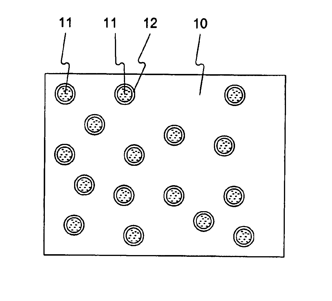
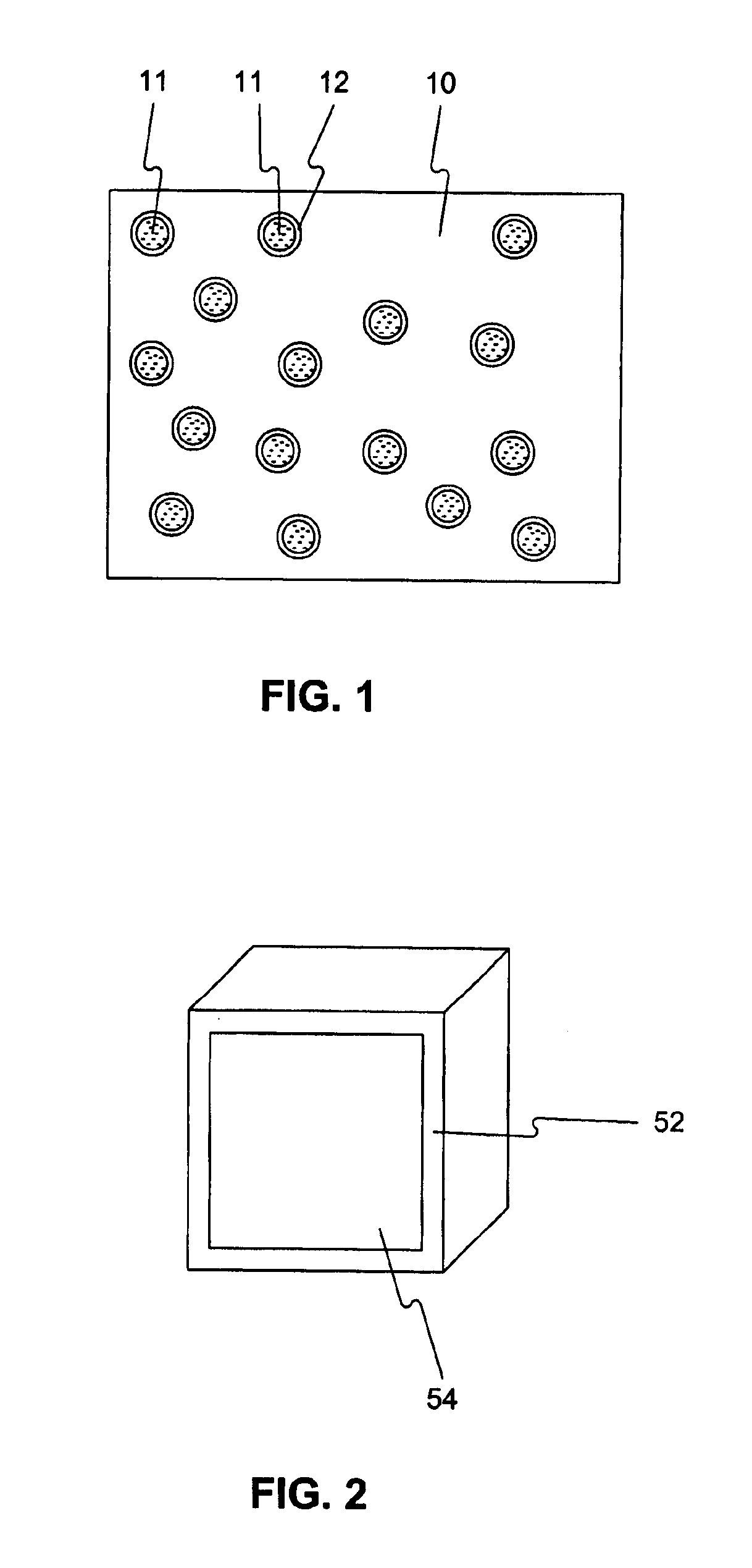
FIG. 1 provides, a schematic representation of a nanocomposite material according to an embodiment of the invention. The nanocomposite material includes a random glassy matrix 10 and plurality of nanoparticles 11 dispersed either uniformly or non-uniformly within matrix 10. While FIG. 1 shows the plurality of nanoparticles 11 including an outer coating layer 12, which at least partially coats nanoparticles 11 and inhibits their agglomeration, depending on the specific properties desired and / or host matri...


PUM

PropertyMeasurementUnit
refractive indexaaaaaaaaaa
radiusaaaaaaaaaa

Abstract

A microresonator is provided that incorporates a composite material comprising a polymer matrix and nanoparticles dispersed therein. The microresonator includes the composite material having a shape that is bounded at least in part by a reflecting surface. The shape of the microresonator allows a discrete electromagnetic frequency to set up a standing wave mode. Advantageously, the polymer matrix comprises at least one halogenated polymer and the dispersed nanoparticles comprise an outer coating layer, which may also comprise a halogenated polymer. Methods for making composite materials and microresonators are also provided. Applications include, for example, active and passive switches, add/drop filters, modulators, isolators, and integrated optical switch array circuits.

Description

FIELD OF THE INVENTIONThe present invention relates to microresonators, such as microrings, microdisks, microspheres, microplates, and microlines made from random glassy matrix materials and nanoparticles distributed within the matrix.BACKGROUNDAll-optical switching between waveguides in dense-wavelength-division multiplexed (hereinafter, “WDM”) networks using microring resonators is well known. However, such switching is limited by optical loss effects. For example, a microring resonator made of an electroabsorptive material coupled to two straight semiconductor side-channel waveguides has been proposed that could operate as a 2×2 crosspoint switch when the rings were switched from a low-absorption state to a high-absorption state. See, Soref et al. “Proposed. N-Wavelength M-Fiber WDM Crossconnect Switch Using Active Microring Resonators”IEEE Phontonics Technology Letters, Vol. 10, No. 8, (August 1998), which is hereby incorporated by reference in its entirety. As described by Sore...

Claims


Application Information

Patent Timeline
Patent Type & Authority Patents(United States)
IPC IPC(8): G02B6/13G02B6/132G02B6/12H02N11/00G02B1/04G02B6/122
CPCB82Y5/00B82Y20/00B82Y30/00H02N11/006G02B6/12007G02B6/1221G02B6/132G02B1/04
Inventor GARITO, ANTHONY F.GAO, RENYUANGAO, RENFENGHSIAO, YU-LINGZHU, JINGSONG
Owner PHOTON
Why Eureka
Try Eureka