Ceramic heater for semiconductor manufacturing and inspecting equipment

a ceramic heater and semiconductor technology, applied in the direction of ohmic-resistance heating, hot plate heating arrangement, electrical equipment, etc., to achieve the effect of accurate temperature measurement of ceramic substra

Inactive Publication Date: 2005-04-12
IBIDEN CO LTD
View PDF15 Cites 8 Cited by
  • Summary
  • Abstract
  • Description
  • Claims
  • Application Information

AI Technical Summary

Benefits of technology

[0029]If the temperature measurement element such as a thermocouple is brought into contact with the ceramic substrate having a surface roughness Ra≦2 μm, the above-mentioned temperature measurement element and the above-mentioned ceramic substrate are brought into almost face contact with each other, so that heat is sufficiently transmitted to the temperature measurement element from the ceramic substrate to make the accurate temperature measurement of the ceramic substrate possible. If Ra>2 μm, the contact with the temperature measurement element becomes a point contact, so that the heat sometimes does not sufficiently transmit to make the accurate temperature measurement impossible. However, in the case Ra is from 2 to 5 μm, the contact surface area can be assured to some extent by transversely laying the temperature measurement element to increase the contact area, so that the temperature measurement error can be corrected.
[0030]To keep the surface roughness Ra at 2 μm or less, it is preferable to keep the surface roughness Ra at 2 μm or less by polishing the surface of the ceramic substrate or forming an insulating layer on the surface of the ceramic substrate.

Problems solved by technology

Further, with respect to the problem that the temperature measurement element of the thermocouple drops during a long time use, the cause is found out that it is owing to the deterioration of a fixing member such as the solder, the inorganic adhesive, and the like by heating.

Method used


Image

  • Ceramic heater for semiconductor manufacturing and inspecting equipment
  • Ceramic heater for semiconductor manufacturing and inspecting equipment
  • Ceramic heater for semiconductor manufacturing and inspecting equipment

Examples


example 1

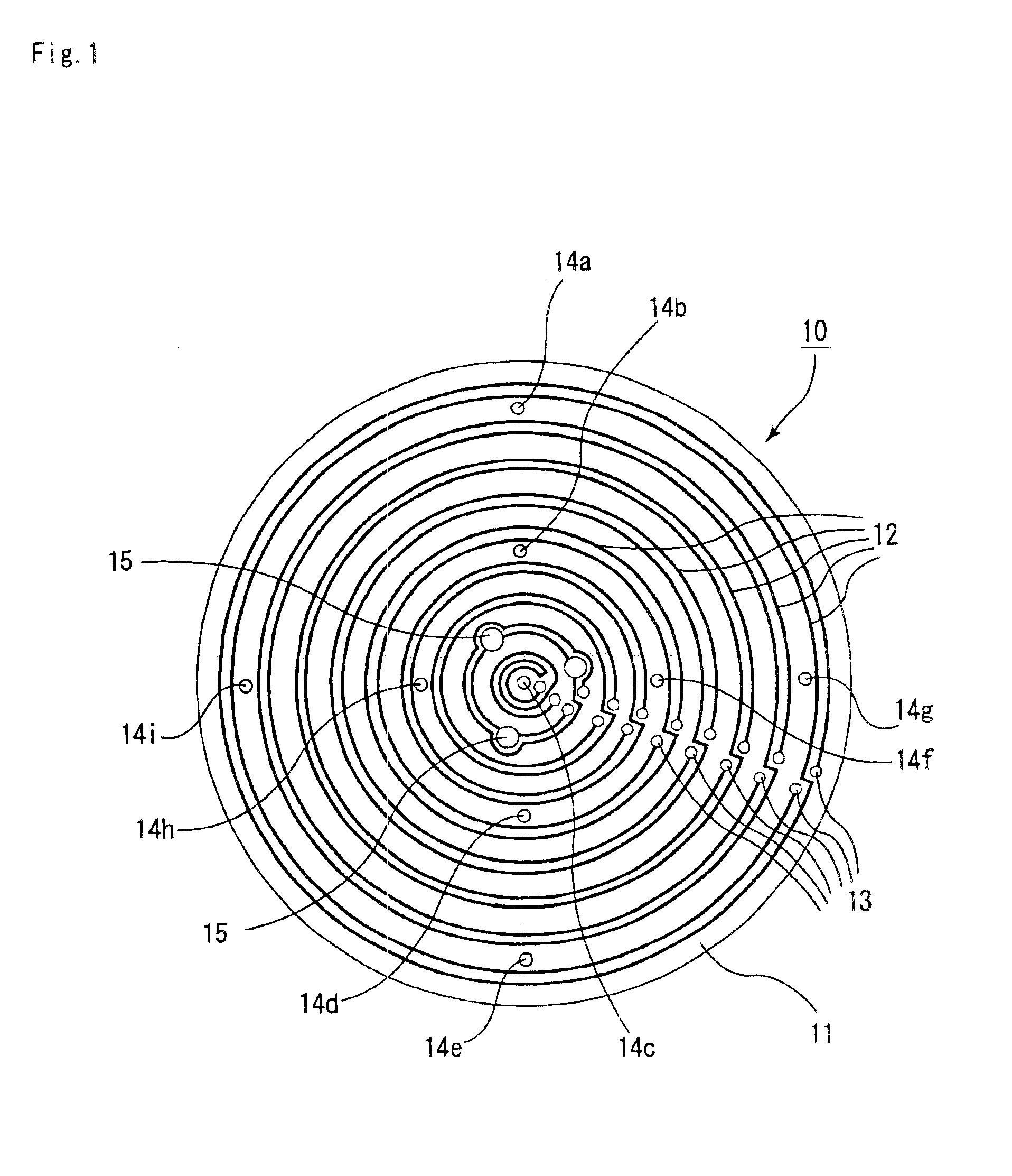
Manufacture of Ceramic Heater Made of Aluminum Nitride (Reference to FIG. 1)

[0216](1) A composition containing 100 parts by weight of an aluminum nitride powder (the average particle diameter: 1.1 μm), 4 parts by weight of yttria (the average particle diameter: 0.4 μm), 12 parts by weight of an acrylic binder, and an alcohol was spray dried to produce a granular powder.

[0217](2) Next, the obtained granular powder was filled in a die and molded to be a flat plate to obtain a raw formed body (a green sheet). The raw formed body was processed by drilling to form through holes 15 to insert lifter pins for a silicon wafer.

[0218](3) On completion of the processing, the raw formed body was hot pressed at 1800° C. and a pressure of 200 kg / cm2 to obtain a 3 mm thick aluminum nitride plate-like body. Next, a disk with a diameter of 12 inch (300 mm) was cut out of the plate-like body to obtain a plate-like body made of ceramic (a ceramic substrate) 11. Further, a glass paste (G-5177 produced b...

example 2

Manufacture of Ceramic Heater Made of Silicon Carbide

[0226]A ceramic heater made of silicon carbide was manufactured in the same manner as Example 1, except that silicon carbide with an average particle diameter of 1.0 μm was used and the sintering temperature was 1900° C. and further, the obtained ceramic substrate surface was fired at 1500° C. for 2 hours to form a 1 μm-thick SiO2 layer on the surface.

[0227]The substrate was ground with a diamond grind stone of #220 at 1 kg / cm2 load and polished with a polishing cloth (Malto Co.) and a diamond paste (particle diameter of 0.25 μm) to adjust the surface roughness to Ra=0.008 μm.

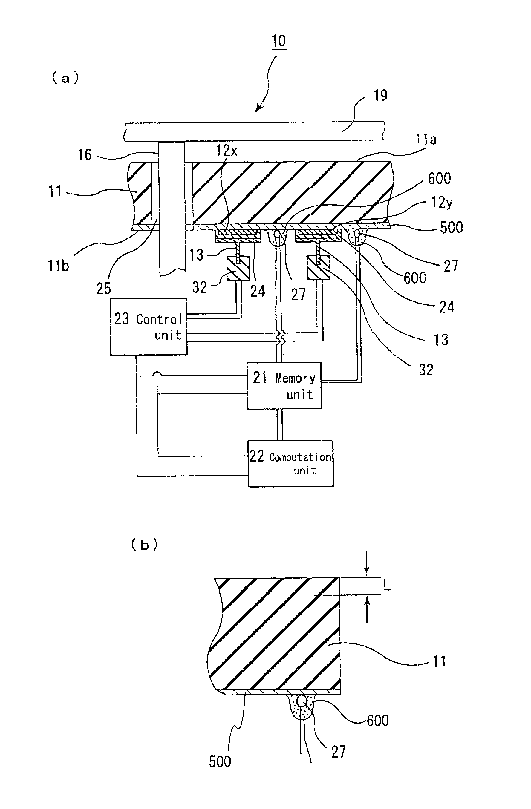
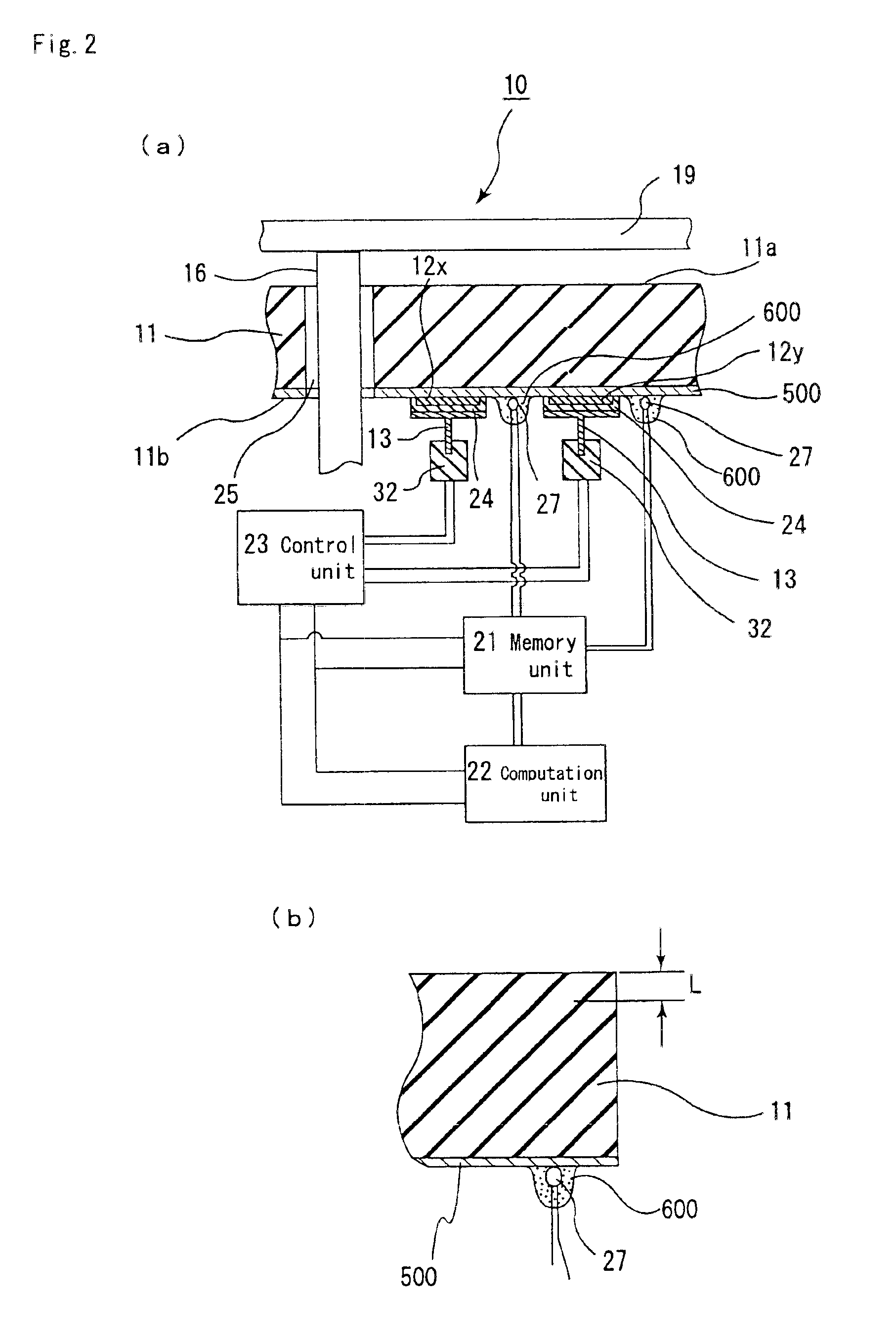
[0228]To the substrate, sheaths S housing thermocouples 44 as shown in FIG. 4 were pushed with springs 45.

example 3

Manufacture of Ceramic Heater Containing Heating Element Inside (Reference to FIG. 3)

[0229](1) Using a paste produced by mixing an aluminum nitride powder (the average particle diameter: 1.1 μm produced by Tokuyama), 4 parts by weight of yttria (the average particle diameter: 0.4 μm), 11.5 parts by weight of an acrylic binder, 0.5 parts by weight of a dispersant, and 53 parts by weight of alcohol consisting of 1-butanol and ethanol, forming was carried out by a doctor blade method to obtain a 0.47 mm green sheet.

[0230](2) Successively, after the green sheet was dried at 80° C. for 5 hours, portions to be through holes 15 with diameters of 1.8 mm, 3.0 mm, and 5.0 mm to insert silicon wafer lifter pins into and portions to be conductor-filled through holes for connection with terminal pins were formed by punching.

[0231](3) Next, a conductor containing paste A was produced by mixing 100 parts by weight of a tungsten carbide particle with an average particle diameter of 1 μm, 3.0 parts ...


PUM

PropertyMeasurementUnit
thicknessaaaaaaaaaa
surface roughness Raaaaaaaaaaa

Abstract

An object of the present invention is to provide a ceramic heater for a semiconductor producing/examining device which is capable of accurately measuring the temperature of an object to be heated and evenly heating the whole body of a silicon wafer by adjusting the heating state of a heating element based on the temperature measurement result, and the ceramic heater for a semiconductor producing/examining device of the present invention is a ceramic heater including a ceramic substrate and a heating element formed on the surface or the inside of the ceramic substrate, wherein a temperature measurement element is formed while being brought into contact with the ceramic substrate and the surface roughness of the ceramic substrate brought into contact with the temperature measurement element is Ra≦5 μm.

Description

TECHNICAL FIELD[0002]The present invention relates to a ceramic heater for a semiconductor producing / examining device, which can be for heating a variety of objects, and more particularly to a ceramic heater for a semiconductor producing / examining device, which can be preferably used for drying, sputtering and the like of a silicon wafer and the like in the semiconductor industry, and which has an excellent temperature evenness of a heating face thereof.BACKGROUND ART[0003]A semiconductor product is produced through several steps including a step of forming a photosensitive resin as an etching resist on a silicon wafer to perform etching for the silicon wafer. This photosensitive resin is liquid-state, so that it is applied onto a surface of the silicon wafer by using a spin coater and the like. However, the photosensitive resin must be dried after applying, and thus the silicon wafer applied with the resin is placed on a heater and heated for drying. Conventionally, a heater used f...

Claims


Application Information

Patent Timeline
Patent Type & Authority Patents(United States)
IPC IPC(8): H01L21/00
CPCH01L21/67248H01L21/67109
Inventor ITO, YASUTAKAITO, ATSUSHI
Owner IBIDEN CO LTD
Why Eureka
Try Eureka