Semiconductor memory having a defective memory cell relieving circuit

a technology of memory cell and relieving circuit, which is applied in the field of semiconductor memory, can solve the problems of large area of the relief circuit, long access time, and defective memory cells, and achieve the effect of avoiding deterioration of characteristics, minimizing the overhead of memory cell arrays, and no overhead

Inactive Publication Date: 2005-04-12
NEC CORP
View PDF27 Cites 14 Cited by
  • Summary
  • Abstract
  • Description
  • Claims
  • Application Information

AI Technical Summary

Benefits of technology

Another object of the present invention is to provide a semiconductor memory which has minimized the area overhead and the access time overhead attributable to the installation of the defective memory cell relief circuit, whereby a semiconductor memory having an elevated chip yield of production and an increased reliability can be obtained.
With the above mentioned arrangement, since the at least one row of substitution information storing memory cells are added to the main memory cells arranged in the form of a matrix having a number of rows and a number of columns, and since only the one row of substitution information storing memory cells store the substitution information, the area overhead of the memory cell array is minimized. In addition, since the substitution information is read out from the substitution information storing memory cells only one time just after a power supply is turned on for the semiconductor memory, it is possible to avoid the characteristics deterioration, of the substitution information storing memory cells which may be formed of the ferroelectric memory cell.
Furthermore, since the substitution of the defective memory cell (namely, the column including the defective memory cell) is completed before the Y selection signal (column selection signal) is supplied to the Y selection circuit, no overhead occurs in the access time.
Therefore, the present invention provides a highly reliable semiconductor memory device having a minimized area overhead and no access time overhead.
Alternatively, the substitution information includes a plurality of bits indicative of an address of one column within the memory cell array excluding the column of redundant memory cells, and an information bit indicative of substitution or non-substitution, and word lines of the memory cell array excluding the row of substitution information storing memory cells are divided into a plurality of groups of word lines, and one substitution information is allocated to each one group of word lines, so that a substitution column can be different from one group of word lines to another group of word lines, whereby even if a plurality of defective memory cells exist in different columns, the defective memory cells can be relieved.

Problems solved by technology

In a process for fabricating a semiconductor memory, defective memory cells occur often, and if the defective memory cells are fount out in an inspecting step, even if only one bit is defective, the whole of the memory chip is rejected.
However, the arrangement disclosed in the above referred JP-A-09-128991 so configured to store the substitution information by action of the ferroelectric memory cells is disadvantageous in that the whole of the relief circuit needs a large area and the access time becomes long.
Therefore, the access time becomes long.
On the other hand, the memory device disclosed in the above referred JP-A-2000-215687 is also disadvantageous in the chip area and in the access time.
In addition, it has another problem in which the characteristics of the ferroelectric capacitor is deteriorated.
Namely, the area overhead attributable to the installation of the redundant circuit is very large.
Furthermore, since the substitution information storing cells are located in the same word lines as those of the main memory cells, the substitution has not yet been achieved at the moment a signal voltage read out from the memory cell has been amplified by a sense amplifier.
Comparing with the case in which the substitution is not carried out, an overhead is inevitably generated in the access time.
In addition, since the substitution information is read out in every memory access, the deterioration in characteristics of the ferroelectric capacitors is unavoidable.
Namely, there is possibility that an erroneous substitution occurs because of the deterioration in characteristics of the substitution information storing cells.

Method used


Image

  • Semiconductor memory having a defective memory cell relieving circuit
  • Semiconductor memory having a defective memory cell relieving circuit
  • Semiconductor memory having a defective memory cell relieving circuit

Examples


third embodiment

The third embodiment is similar to the first and second embodiments in the reading of the substitution information storing memory cells and in that in a second and succeeding cycles, the main memory cells are accessed and the substitution information storing memory cells are not accessed.

The selection of the substitution information read out from the substitution information storing memory cells RMC0 to RMC63 become possible when the X address becomes established. Therefore, the decoder DEC starts to operate at the moment the word lines WLx are activated.

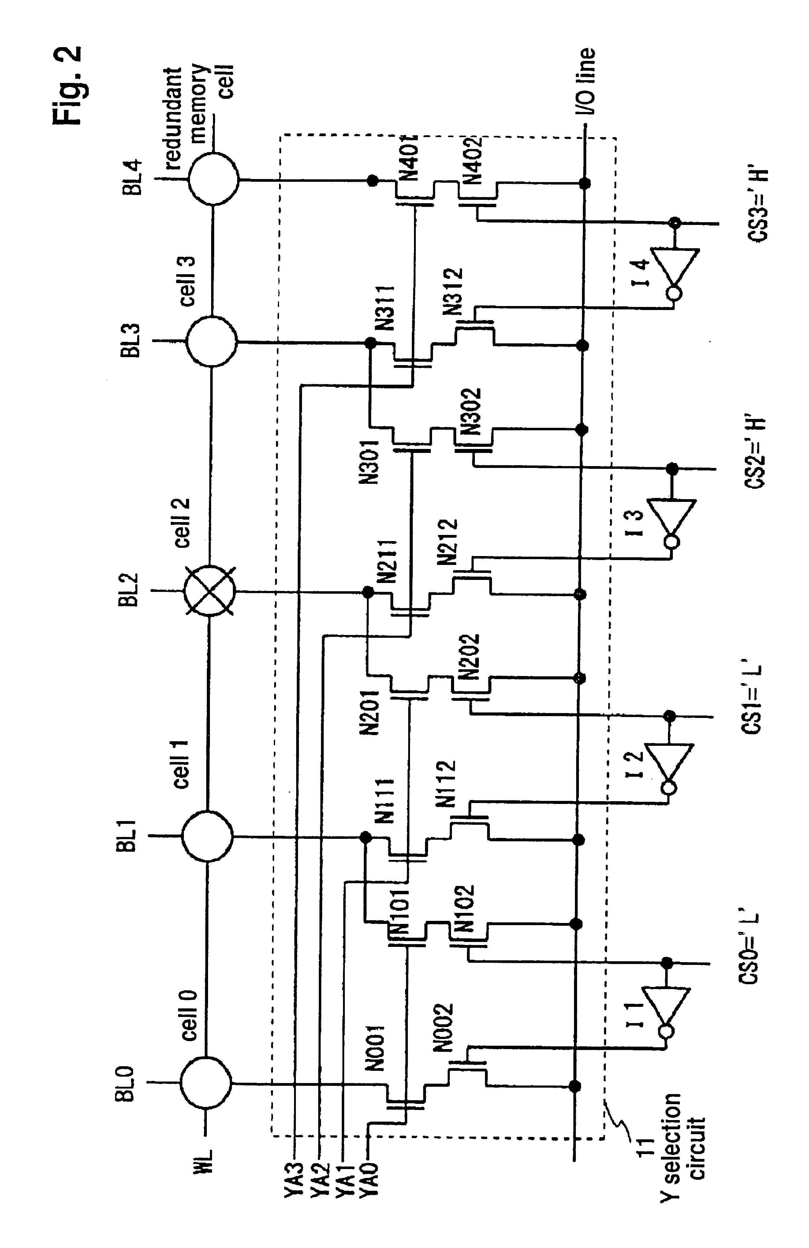
On the other hand, if the Y selection signal is brought to the high level “H”, the data read out from the memory cell is outputted through the I / O line to the external, or the write data supplied from the external is written into the memory cell through the I / O line, and when the Y selection signal is returned to the low level “L”, the control circuit 12A terminates the operation.

Therefore, the time after the word line is brought to...

fourth embodiment

Now, a fourth embodiment of the semiconductor memory in accordance with the present invention will be described. Referring to FIG. 11, there is shown a block diagram of the semiconductor memory in accordance with the present invention.

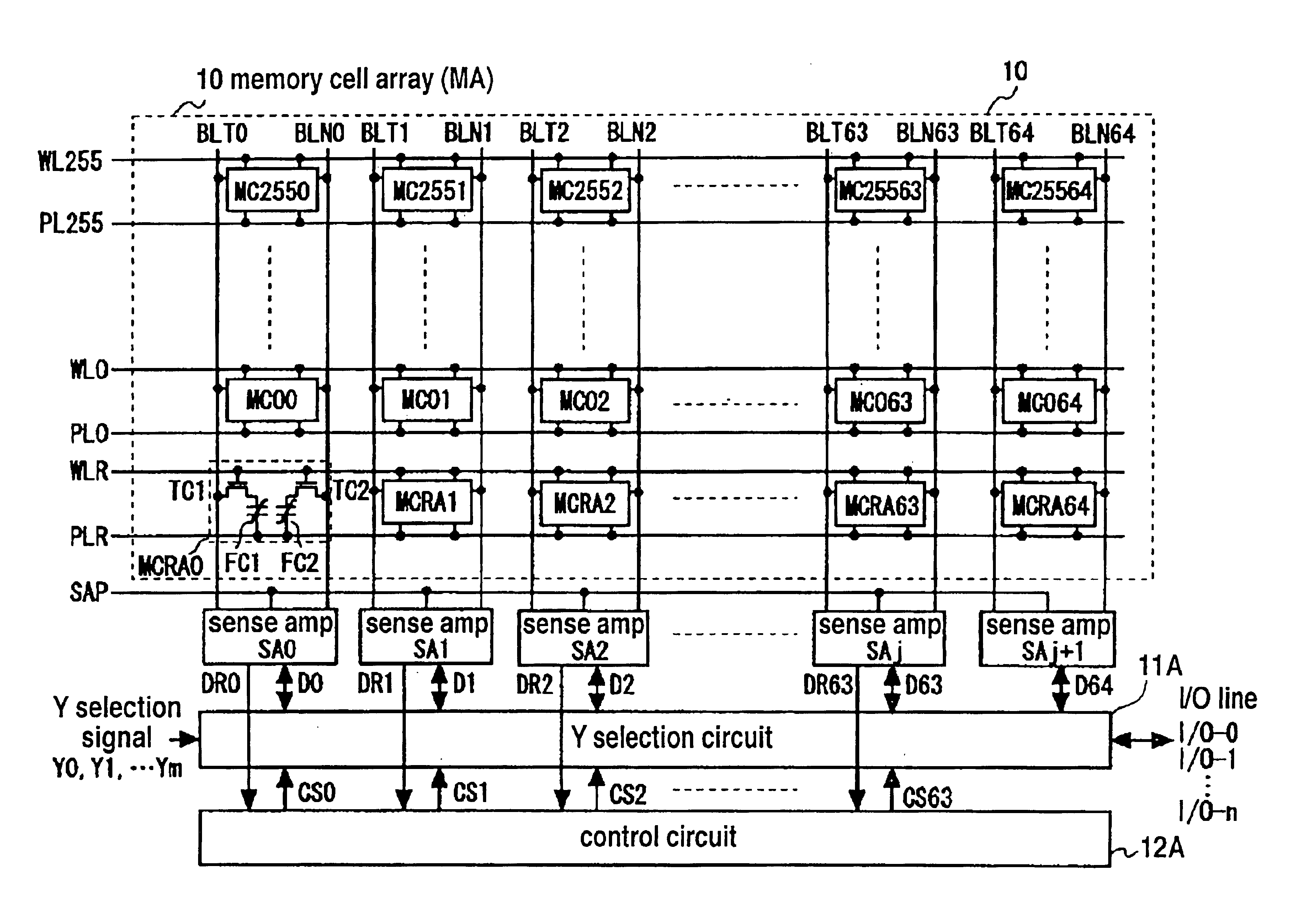
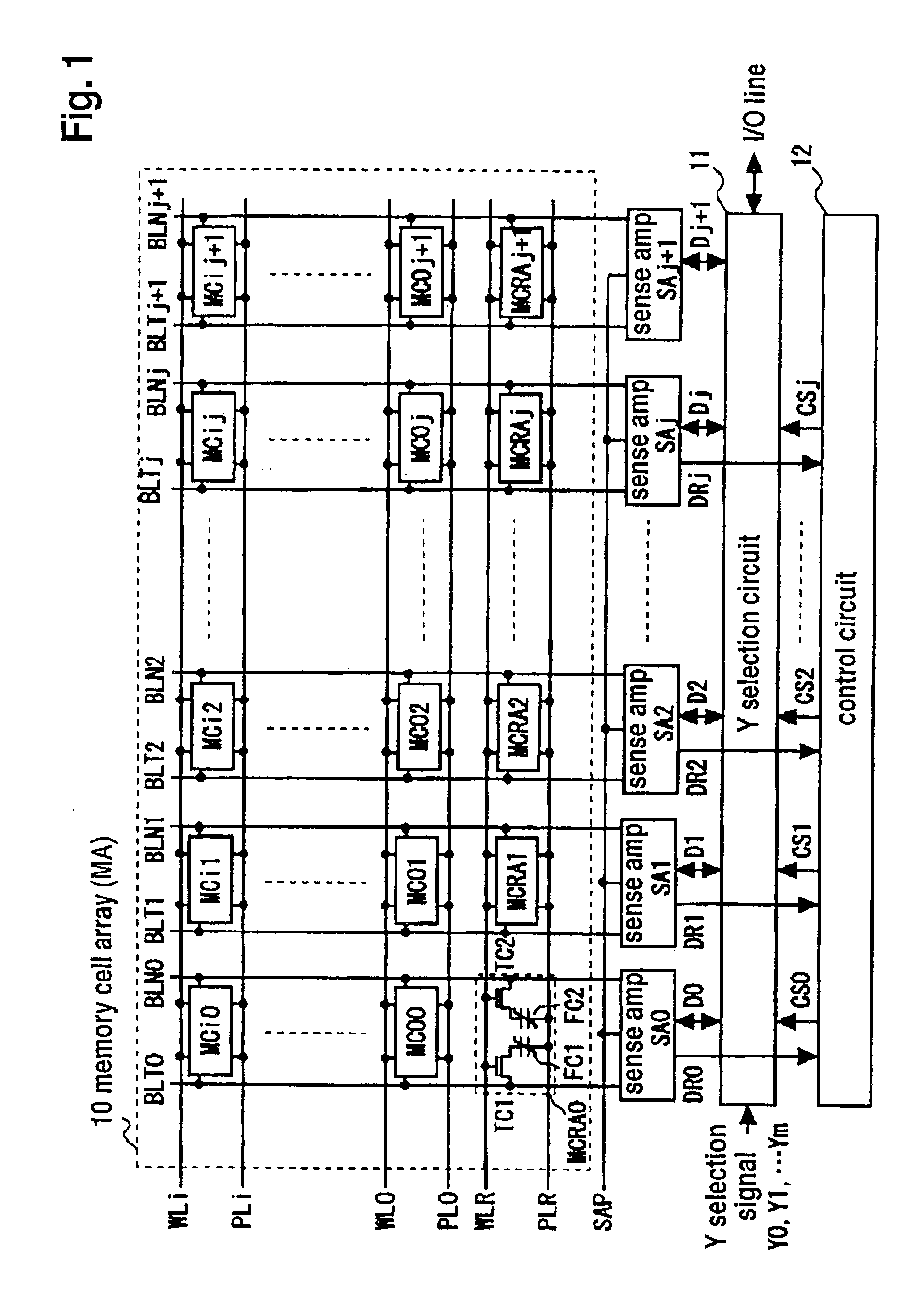
The shown fourth embodiment includes two sub-arrays “subarray0” and “subarray1”. The “subarray0” includes a memory cell array MA1 and a plurality of sense amplifiers SA0 to SAj+1. The memory cell array MA1 includes a number of memory cells MC00 to MCij, one column of redundant memory cells MC0j+1 to MCij+1, and one word line of substitution information storing memory cells MCR0 to MCRAj+1.

Furthermore, transfer gates TG00 and TG10 to TG0j+1 and TG1j+1 are inserted between the substitution information storing memory cells and the memory cells MC00 to MCij and the redundant memory cells MC0j+1 to MCij+1, and controlled by a signal ETG to be able to selectively separate the memory cells MC00 to MCij and the redundant memory cells MC0j+1 to MCij+1, from the...

sixth embodiment

Now, a sixth embodiment of the semiconductor memory device in accordance with the present invention will be described with reference to FIG. 8, which is a block diagram of the semiconductor memory device. In FIG. 18, elements corresponding to those shown in FIG. 5 are given the same reference numbers, and explanation will be omitted for simplification of the description.

In this sixth embodiment, a memory cell array (MA2) 10 includes a number of memory cells MC00 to MCij arranged in the form of a matrix and one column of redundant memory cells MC0j+1 to MCij+1, but does not include substitution information storing memory cells.

Each of sense amplifiers SA0 to SAj+1 is connected to a corresponding pair of bit lines of a number of bit lines pairs BLT0 and BLN0 to BLTj+1 and BLNj+1. A Y selection circuit 11A is the same as the construction shown in FIG. 6.

A control circuit 12B is constituted of “j+1” non-volatile memory cells arranged for example as shown in FIG. 19. As shown in FIG. 19,...


PUM


Abstract

In a semiconductor memory incorporating therein a circuit for relieving a defective memory cell, a memory cell array constituted of a number of main memory cells MC00 to MCij is added with one column of redundant memory cells MC0j+1 to MCij+1 and one word line of substitution information storing memory cells MCRA0 to MCRAj+1. In only a first cycle after the power supply is turned on, the substitution information DR0 to DRj is read out from the substitution information storing memory cells by use of a writing / reading circuit associated with the main memory cells, and is transferred to and held in a control circuit. In a second and succeeding cycles, the control circuit generates Y selection circuit control signals CS0 to CSj on the basis of the substitution information held in the control circuit, and a Y selection circuit is controlled by the control signals CS0 to CSj so as to selectively connect the columns other than a defective column to an input / output line. Thus, a chip area overhead attributable to the installation of the defective memory cell relief circuit is minimized. In addition, an address comparing circuit for a defective memory cell substitution is no longer necessary, and an access time overhead attributable to the address substitution operation does not occur.

Description

BACKGROUND OF THE INVENTIONThe present invention relates to a semiconductor memory, and more specifically to a method for relieving a defective memory cell and a semiconductor memory incorporating therein a circuit for relieving a defective memory cell.In a process for fabricating a semiconductor memory, defective memory cells occur often, and if the defective memory cells are fount out in an inspecting step, even if only one bit is defective, the whole of the memory chip is rejected. Therefore, particularly, in a semiconductor memory having a large memory capacity, redundant memory cells are previously provided to relieve the defective cells. In order to relieve the defective cells, it is necessary to provide on a chip a non-volatile memory for storing information for substituting a nondefective redundant memory cell for the defective memory cell found out in a chip test time.In the prior art, in many cases, a memory of the information for substituting the nondefective redundant me...

Claims


Application Information

Patent Timeline
Patent Type & Authority Patents(United States)
IPC IPC(8): G11C29/00G11C29/04
CPCG11C29/848G11C29/789G11C11/22
Inventor YAMADA, JUNICHI
Owner NEC CORP
Why Eureka
Try Eureka