Carrier for cleaning sockets for semiconductor components having contact balls

a technology of contact balls and sockets, which is applied in the direction of cleaning using liquids, instruments, lighting and heating apparatus, etc., can solve the problems of difficult to make low-resistance electrical connections with deformed contact balls, the material of the socket is relatively soft, and the ball deforms easily, etc., to achieve low resistance, resist wear, deformation, and oxide buildup

Inactive Publication Date: 2005-04-19
MICRON TECH INC
View PDF30 Cites 1 Cited by
  • Summary
  • Abstract
  • Description
  • Claims
  • Application Information

AI Technical Summary

Benefits of technology

[0013]The test carrier can be configured for testing bare dice, chip scale packages, BGA devices, or wafers. During test procedures using the test carrier, the contact members on the base make low resistance electrical connections with the contact balls on the components, and protect the contact balls from deformation. In addition, the terminal contacts on the base make low resistance electrical connections with electrical connectors of a test socket, and resist wear, deformation, and oxide build up even with continued usage in a production environment.

Problems solved by technology

One problem with solder contact balls is that solder is a relatively soft material, and the balls deform easily during handling and testing of the components.
This problem is compounded during testing at elevated temperatures, such as burn-in testing, as heating further softens the solder.
For performing subsequent test procedures, it may be difficult to make low resistance electrical connections with deformed contact balls.
In particular, the electrical connectors on the test apparatus may not adequately engage the surfaces of the contact balls.
Also, for subsequent bonding procedures, deformed balls can make alignment and bonding of the component with a mating substrate more difficult to perform.
In addition, deformed contact balls are a cosmetic problem that can affect a users perception of a semiconductor component.
In addition to making electrical connections for test procedures more difficult, deformed contact balls can alter test results by affecting electrical characteristics, such as contact resistance, inductance, and signal speed during the test procedure.
Further, solder readily oxidizes, which adds resistance to the electrical connections with the contact balls.
Another problem with solder contact balls is the adverse affect that solder can have on a semiconductor test system.
For example, solder flakes can break loose from the balls, contaminating test sockets, and other electrical components associated with the test system.
This can change the calibration of the test system and affect test results on all of the components being tested.
In addition, solder is a contaminant to other semiconductor fabrication processes, and its presence requires special handling and segregation of the components.

Method used


Image

  • Carrier for cleaning sockets for semiconductor components having contact balls
  • Carrier for cleaning sockets for semiconductor components having contact balls
  • Carrier for cleaning sockets for semiconductor components having contact balls

Examples


Embodiment Construction

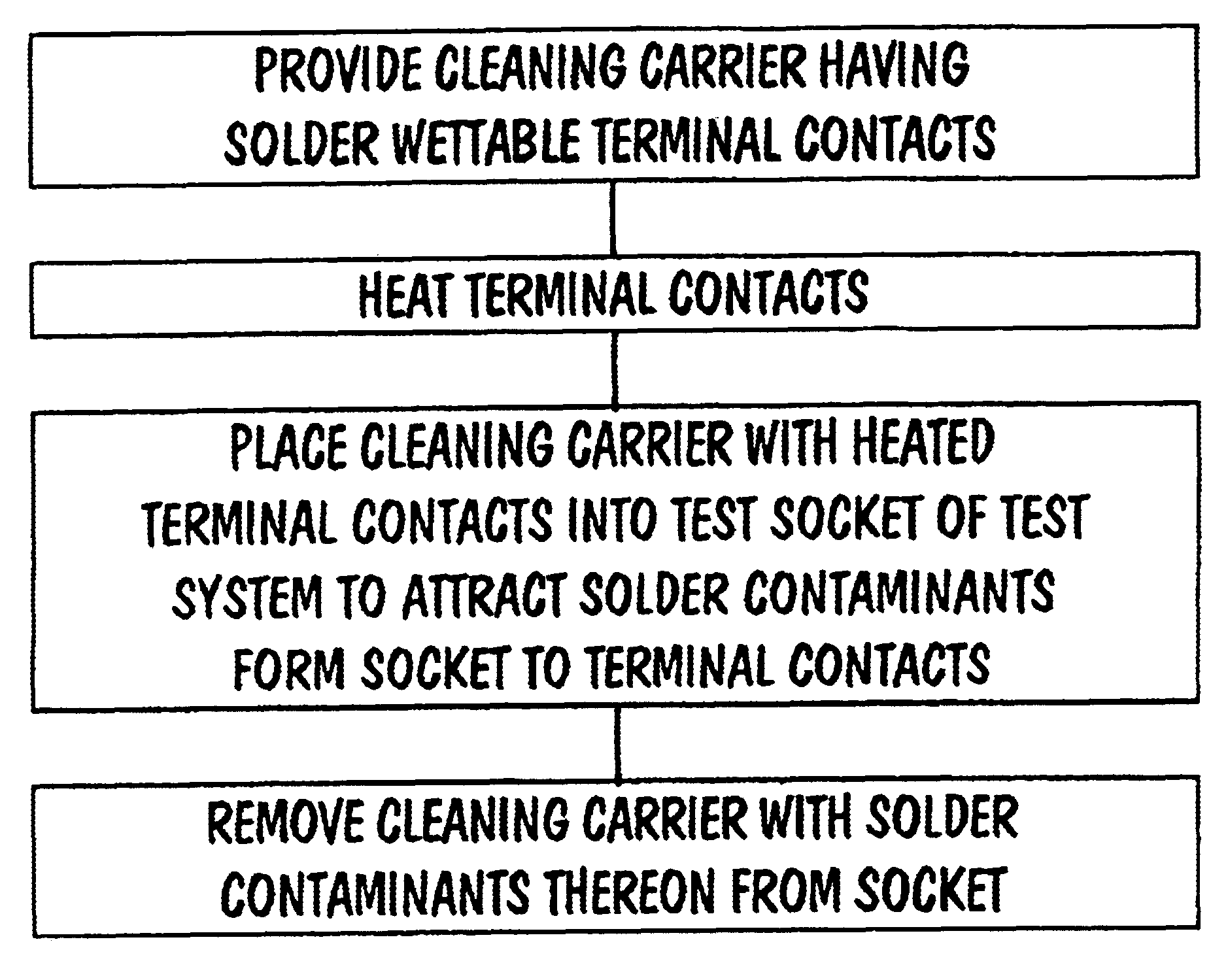
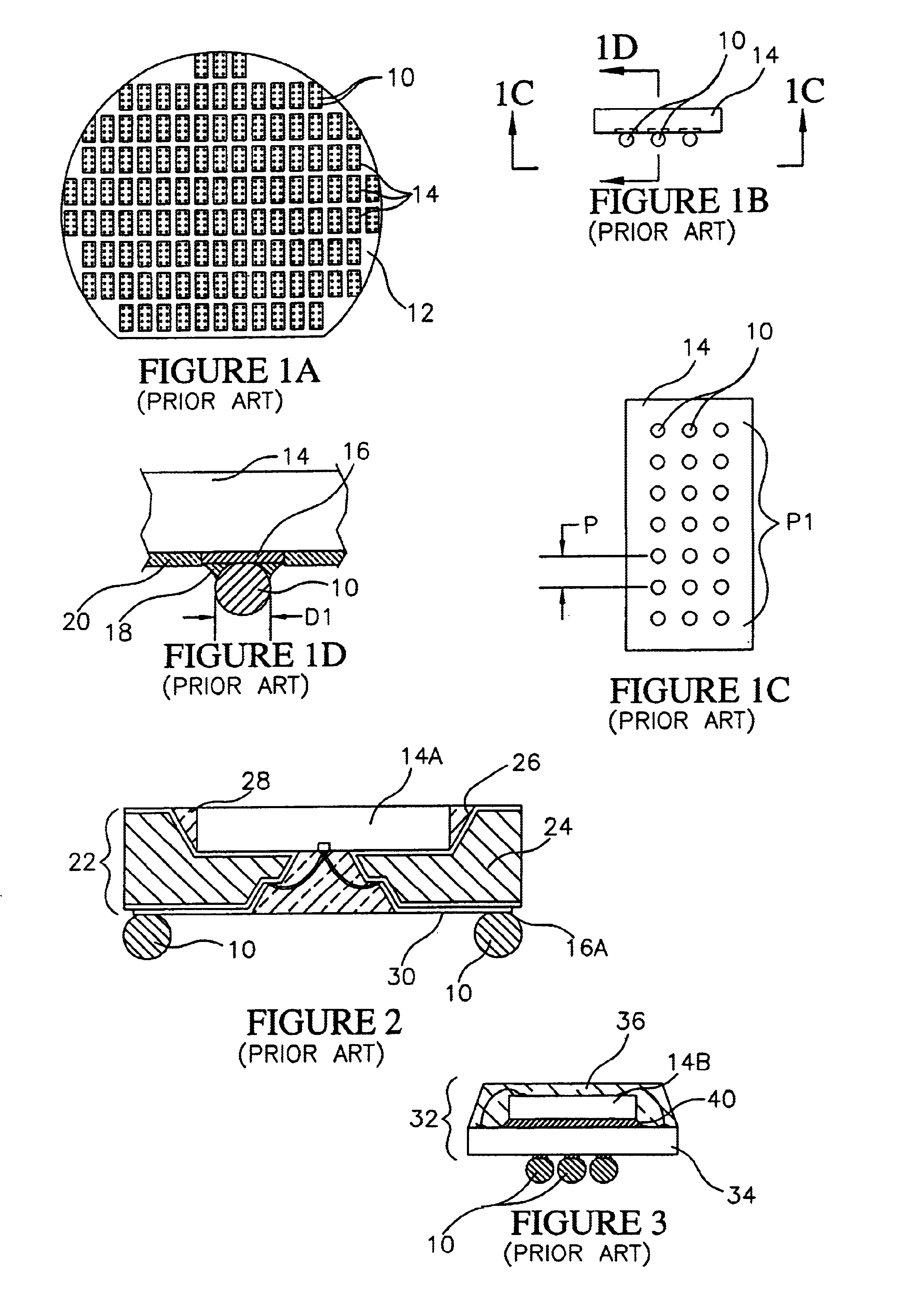
[0045]Referring to FIGS. 1A-1D, 2, and 3, various prior art semiconductor components having contact balls 10 are illustrated.

[0046]In FIG. 1A, a semiconductor wafer 12 comprises a plurality of semiconductor dice 14. FIG. 1B illustrates a die 14 that has been separated from the wafer 12. Each die 14 includes a plurality of contact balls 10. As will be further explained, test carriers can be constructed in accordance with the invention for testing either the wafer 12, or the die 14.

[0047]As shown in FIG. 1C, the contact balls 10 are formed on the die 14 in a pattern P1. In the illustrative embodiment, the pattern P1 is a dense grid array, such as a ball grid array (BGA). By way of example, a representative diameter D1 for the contact balls 10 can be about 0.005-in (0.127 mm) to 0.050-in (1.270 mm) or greater. A representative pitch P (center to center spacing) of the contact balls 10 can be from about 0.008-in (0.228 mm) to about 0.060-in (1.524 mm) or greater.

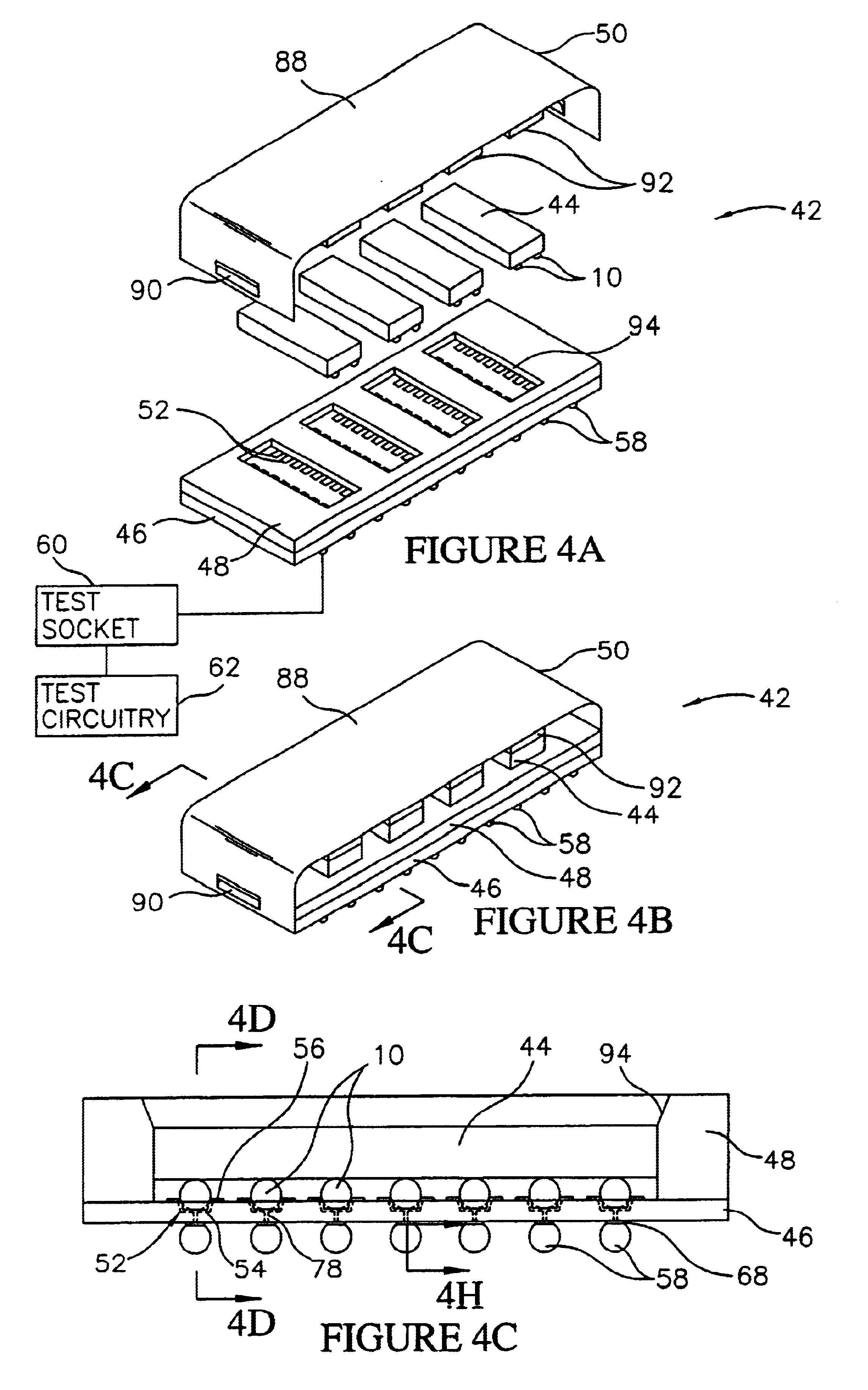
[0048]The die 14 also in...


PUM


Abstract

A test carrier for testing bumped semiconductor components such dice, chip scale packages, BGA devices, and wafers is provided. The test carrier includes a base for retaining one or more components and contact members for making temporary electrical connections with contact balls on the components (e.g., solder balls). The test carrier also includes terminal contacts formed as hard metal balls, as hard metal balls coated with a non-oxidizing metal layer, or as glass, ceramic or plastic members coated with a conductive material. The contact members on the base protect the contact balls on the components from deformation during testing and handling. The terminal contacts on the test carrier are configured for multiple uses in a production environment without deformation.
Also provided is a calibration carrier for calibrating semiconductor test systems for bumped components, and a cleaning carrier for cleaning test sockets for bumped components. The calibration carrier can include on board evaluation circuitry for evaluating electrical characteristics of a test system, such as contact resistances between electrical connectors of a test socket and terminal contacts on the calibration carrier. The cleaning carrier includes terminal contacts formed of a solder wettable material configured to attract solder contaminants in test sockets.

Description

CROSS REFERENCE TO RELATED APPLICATIONS[0001]This application is a division of Ser. No. 09 / 621,121, filed on Jul. 21, 2000, now U.S. Pat. No. 6,504,389 which is a division of Ser. No. 09 / 146,715, filed on Sep. 3, 1998, U.S. Pat. No. 6,208,156 B1.FIELD OF THE INVENTION[0002]This invention relates generally to the manufacture and testing of semiconductor components. More particularly, this invention relates to systems and carriers for testing bumped semiconductor components such as bare semiconductor dice, chip scale packages, BGA devices, and semiconductor wafers, having contact balls.BACKGROUND OF THE INVENTION[0003]Semiconductor components, such as bare dice, chip scale packages, BGA devices and wafers can include terminal contacts in the form of contact balls. This type of component is sometimes referred to as a “bumped” component (e.g., bumped die, bumped wafer).[0004]The contact balls provide a high input / output capability for a component, and permit the component to be surface ...

Claims


Application Information

Patent Timeline
Patent Type & Authority Patents(United States)
IPC IPC(8): G01R1/02G01R1/04H05K3/32H05K1/11G01R3/00
CPCG01R1/0483H05K3/325H01L2924/01087H01L2224/16H01L2224/4824H01L2924/01004H01L2924/01046H01L2924/01077H01L2924/01078H01L2924/01079H01L2924/09701H01L2924/14H01L2924/15311H01L2924/30107H05K1/112G01R3/00H01L24/05H01L2224/05568H01L2224/05571H01L2224/05573H01L2224/05624H01L2924/00014
Inventor HEMBREE, DAVID R.
Owner MICRON TECH INC
Why Eureka
Try Eureka