Method for fabricating metal silicide

a metal silicide and polysilicon technology, applied in the direction of vacuum evaporation coating, chemical vapor deposition coating, coating, etc., can solve the problems of undesirable adhesion between the metal silicide and the polysilicon layer, adversely affecting the operating speed, and high rc delay

Inactive Publication Date: 2005-04-26
MACRONIX INT CO LTD
View PDF5 Cites 0 Cited by
  • Summary
  • Abstract
  • Description
  • Claims
  • Application Information

AI Technical Summary

Benefits of technology

[0006]Accordingly, the present invention provides a fabrication method for metal silicide, wherein the formation of a native oxide layer on a polysilicon layer is prevented.
[0007]The present invention provides a fabrication method for metal silicide, wherein the adhesion between metal silicide and the polysilicon layer is enhanced.
[0010]Since a nitrogen-containing adhesion layer is formed on the surface of the conductive layer, the generation of a native oxide layer is thus suppressed by the adhesion layer. The adhesion between the subsequently formed metal silicide layer and the conductive layer is thus desirable and the problem of peeling is prevented.

Problems solved by technology

The contact resistance of the gate and the conductive line in the device thereby increases, leading to a higher RC delay and adversely affecting the operating speed.
Therefore, as the semiconductor wafer is being subjected to the thermal process for forming metal silicide, the adhesion between the metal silicide and the polysilicon layer is undesirable due to the presence of the native oxide layer.
Metal silicide is easily peeled off the polysilicon layer, adversely affecting the reliability and the effectiveness of the device.

Method used


Image

  • Method for fabricating metal silicide
  • Method for fabricating metal silicide
  • Method for fabricating metal silicide

Examples


Embodiment Construction

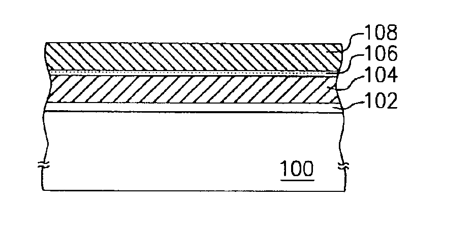
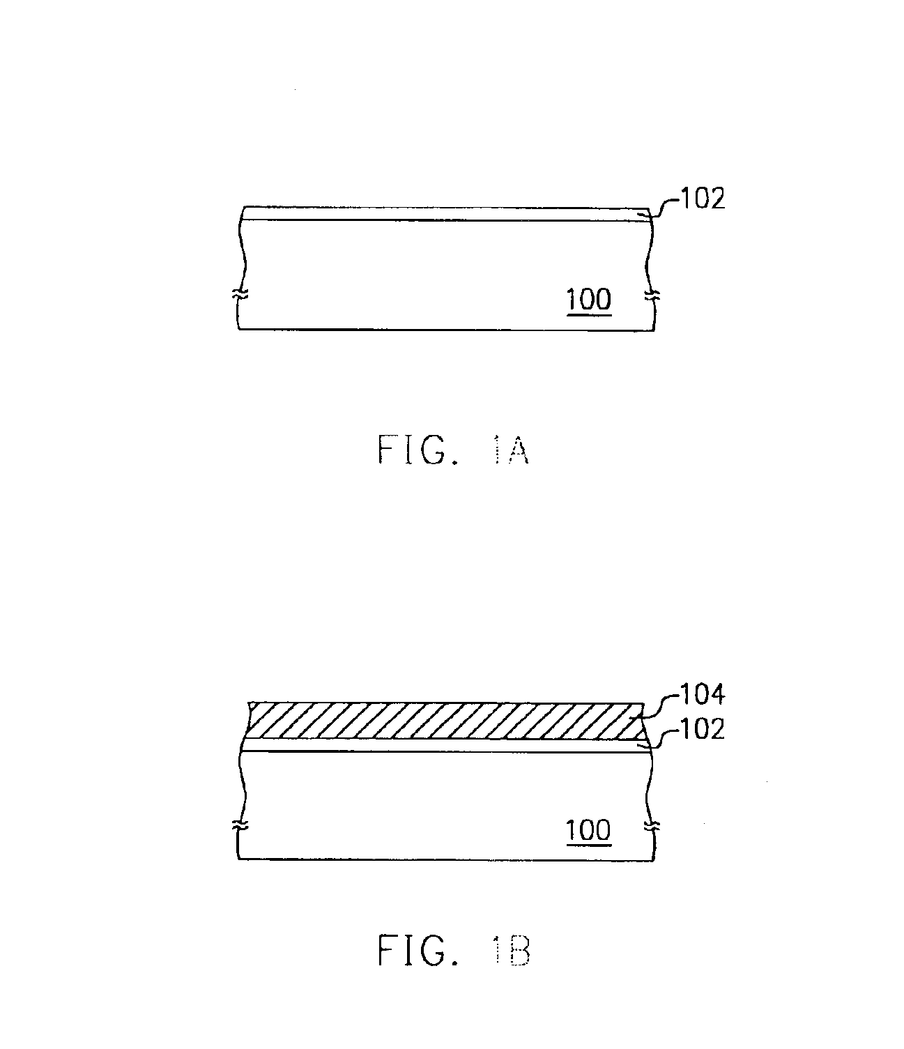
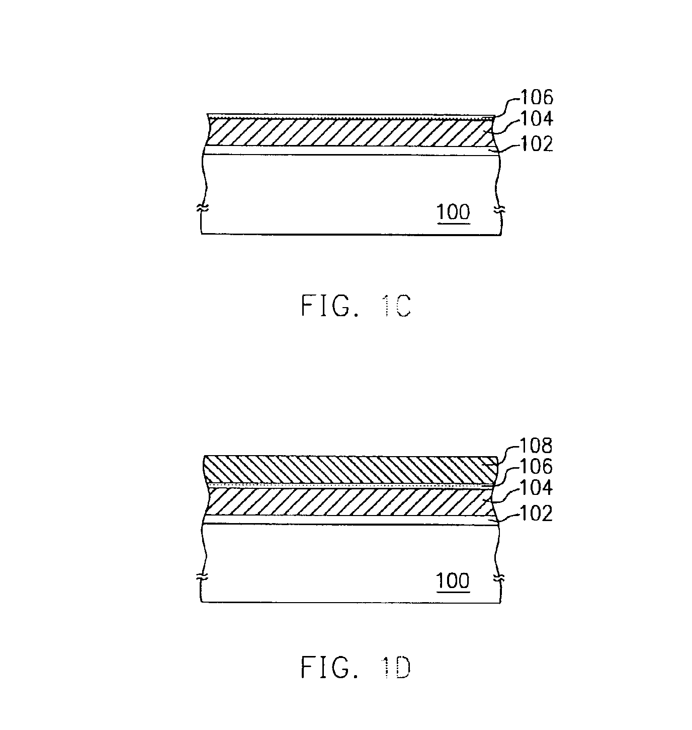
[0015]FIGS. 1A to 1D are schematic cross-sectional views illustrating the process flow for fabricating metal silicide according to the first aspect of the present invention.

[0016]Referring to FIG. 1A, a dielectric layer 102 is provided over a substrate 100, wherein the dielectric layer 102 is formed with a material, such as, silicon oxide. The dielectric layer 102 is formed by, for example, thermal oxidation. This dielectric layer 102 is used as, for example, the gate dielectric layer of the semiconductor device.

[0017]Referring to FIG. 1B, a conductive layer 104 is formed on the dielectric layer 102, wherein the conductive layer 104 is formed with, for example, doped polysilicon. Forming the conductive layer 104 is by, for example, performing an in-situ ion doping using chemical vapor deposition (CVD) to form a doped polysilicon layer on the substrate 100. This conductive layer 104 serves as, for example, the gate of the semiconductor device.

[0018]Continuing to FIG. 1C, an adhesion ...


PUM

PropertyMeasurementUnit
thicknessaaaaaaaaaa
thickaaaaaaaaaa
thickaaaaaaaaaa

Abstract

A method for fabricating a metal silicide layer includes forming a dielectric layer on a substrate, followed by forming a polysilicon material conductive layer on the dielectric layer. An adhesion layer is then formed on the conductive layer, wherein the adhesion layer is a nitrogen rich layer or a nitrogen ion implanted layer. A metal silicide layer is then formed on the adhesion layer. The adhesion between the metal silicide layer and the conductive layer is more desirable due the adhesion layer.

Description

BACKGROUND OF INVENTION[0001]1. Field of Invention[0002]The present invention relates to a method for fabricating a semiconductor device. More particularly, the present invention relates to a method for fabricating metal silicide on polysilicon.[0003]2. Description of Related Art[0004]As the integration of semiconductor device increases, the pattern and the line width in the device gradually decrease. The contact resistance of the gate and the conductive line in the device thereby increases, leading to a higher RC delay and adversely affecting the operating speed. Since the resistance of metal silicide is lower than polysilicon and the thermal stability of metal silicide is higher than a typical inter-metal dielectric material, forming metal silicide on a gate can lower the resistance between the gate and the metal interconnect.[0005]During the conventional fabrication method for metal silicide, after a polysilicon layer, for example, a gate, is formed on a semiconductor wafer and b...

Claims


Application Information

Patent Timeline
Patent Type & Authority Patents(United States)
IPC IPC(8): H01L21/70H01L21/28H01L21/02H01L21/768H01L29/49H01L29/40
CPCH01L21/28044H01L29/4941H01L21/28061
Inventor CHANG, KENT KUOHUA
Owner MACRONIX INT CO LTD
Why Eureka
Try Eureka