Exposure apparatus and method of manufacturing a semiconductor device using the same

a technology of semiconductor devices and exposure apparatus, which is applied in the direction of photomechanical equipment, printers, instruments, etc., can solve the problems of reducing the efficiency of the optical system, and only using the fluorine excimer laser in an environment, so as to prevent any adverse effect on the precision of stage alignment and easy purge only the minimum spaces

Inactive Publication Date: 2005-04-26
CANON KK
View PDF13 Cites 9 Cited by
  • Summary
  • Abstract
  • Description
  • Claims
  • Application Information

AI Technical Summary

Benefits of technology

[0016]The present invention has been made to overcome the conventional drawbacks, and has as its object to provide an exposure apparatus which can easily purge only minimum spaces near a wafer and reticle, and provide a purge structure capable of preventing any adverse effect on the stage alignment precision.

Problems solved by technology

Thus, the fluorine excimer laser can only be used in an environment in which the atmospheric pressure is decreased to almost vacuum and the oxygen concentration is fully decreased.
In addition, various products generated by ozone are deposited on the surface of an optical element, decreasing the efficiency of the optical system.
However, oxygen and moisture cannot be satisfactorily purged (see, e.g., Japanese Patent Laid-Open No. 6-260385).
However, this method is not practical because it is difficult to move the stage (e.g., Japanese Patent Laid-Open No. 8-279458).
If a purge chamber is installed on the floor to purge the overall exposure apparatus including these units, the purged space is contaminated or the oxygen concentration decreases due to a substance vaporized from the units and air which leaks from the air compressors.
When the purge chamber is arranged on the exposure apparatus main body supported by a vibration isolating mechanism, vibrations of the panel of the box-like purge chamber made of a metal thin plate or the like are mixed as noise in the signal of a laser interferometer used for stage alignment on the exposure apparatus main body, adversely affecting the stage alignment precision.
It is difficult to partially seal these spaces.

Method used


Image

  • Exposure apparatus and method of manufacturing a semiconductor device using the same
  • Exposure apparatus and method of manufacturing a semiconductor device using the same
  • Exposure apparatus and method of manufacturing a semiconductor device using the same

Examples


Embodiment Construction

[0054]A preferred embodiment of the present invention will be described in detail below with reference to the accompanying drawings.

[0055]An exposure apparatus according to the present invention is not limited to the contents of the following embodiment, and is applied to a known exposure apparatus as far as a mask pattern is transferred onto a photosensitive substrate via a projection optical system by using ultraviolet rays as exposure light.

[0056]Ultraviolet rays as exposure light used in the exposure apparatus of the present invention are not limited. As described in the BACKGROUND OF THE INVENTION section, the present invention is effective for far ultraviolet rays, particularly, an ArF excimer laser beam with a wavelength around 193 nm and a fluorine (F2) excimer laser beam with a wavelength around 157 nm.

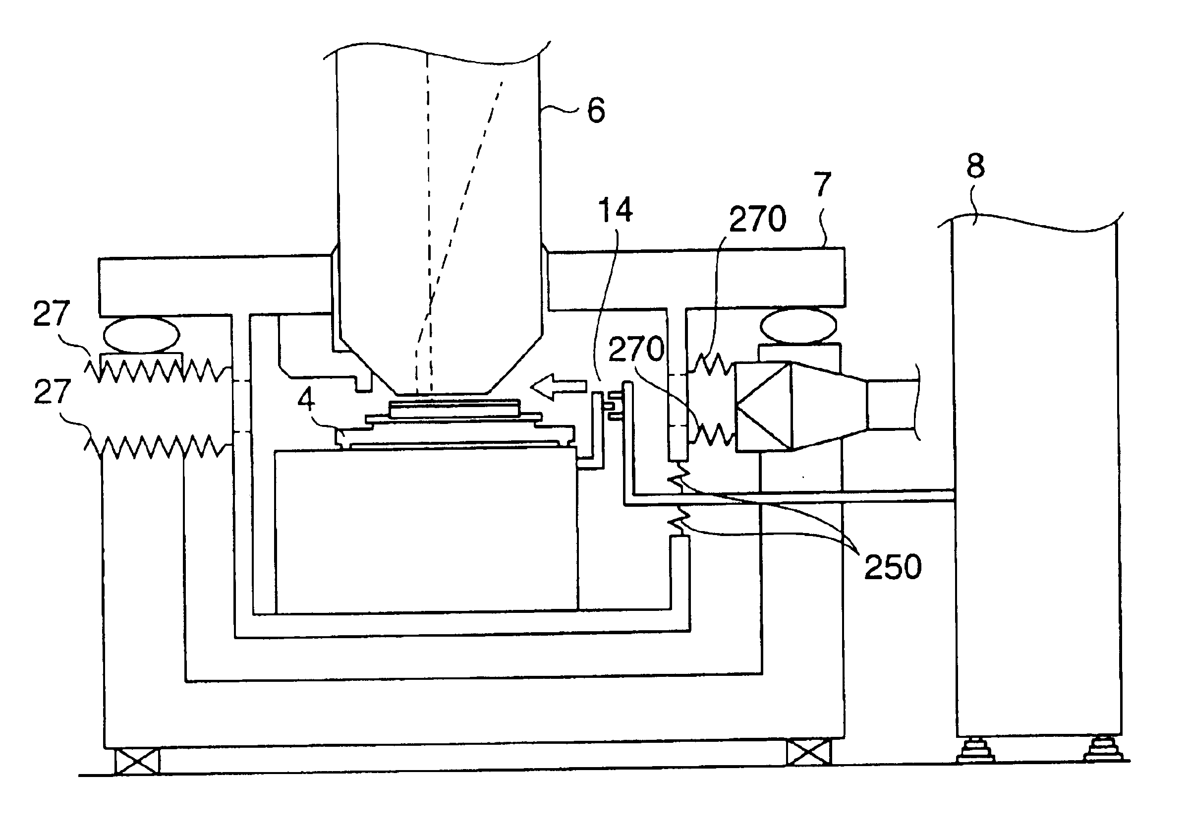
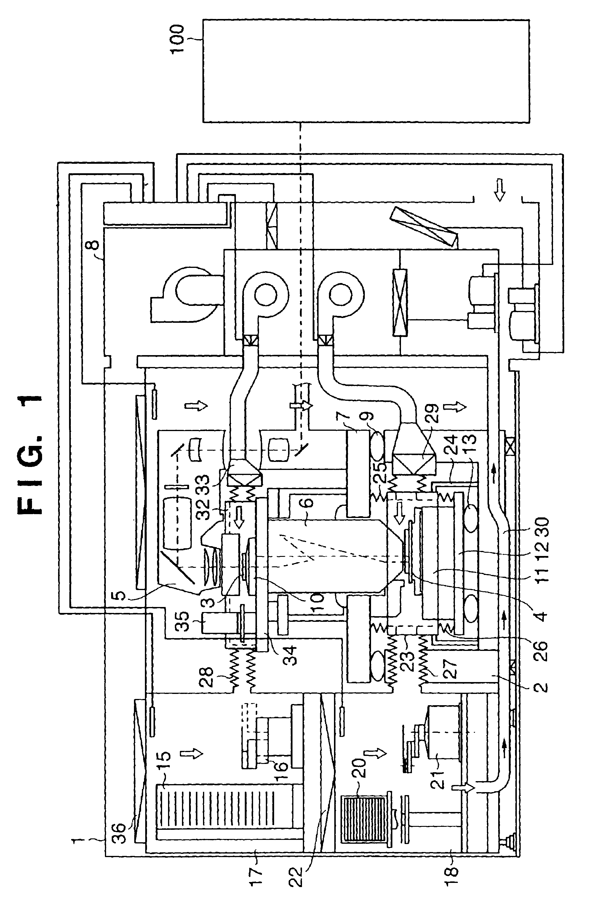
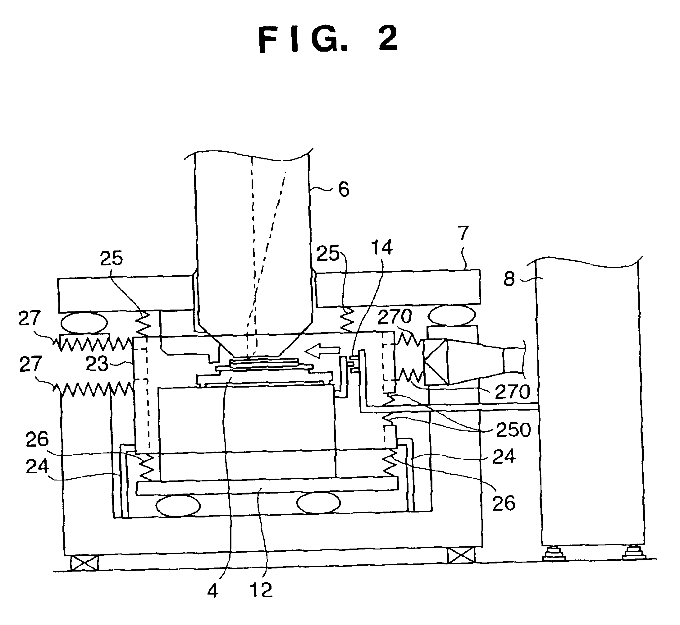
[0057]The embodiment of the present invention will be described with reference to FIG. 1.

[0058]FIG. 1 is a schematic view showing a semiconductor device manufacturing exposur...


PUM

PropertyMeasurementUnit
oscillation wavelengthaaaaaaaaaa

Abstract

An exposure apparatus has a structure supported by a vibration isolating mechanism and a partition wall inserted in at least part of the optical path of exposure light used in the exposure apparatus. The structure and partition wall are coupled by an elastic seal member to form a closed space, and the interior of the partition wall is partitioned from the remaining space.

Description

FIELD OF THE INVENTION[0001]The present invention relates to an exposure apparatus which transfers a mask pattern onto a photosensitive substrate via a projection optical system.BACKGROUND OF THE INVENTION[0002]A conventional manufacturing process for a semiconductor element such as an LSI or VLSI formed from a micropattern uses a reduction type projection exposure apparatus for printing and forming by reduction projection a circuit pattern drawn on a mask onto a substrate coated with a photosensitive agent. With an increase in the packaging density of semiconductor elements, demands have arisen for further micropatterning. Exposure apparatuses are coping with micropatterning along with the development of a resist process.[0003]A means for increasing the resolving power of the exposure apparatus includes a method of changing the exposure wavelength to a shorter one, and a method of increasing the numerical aperture (NA) of the projection optical system.[0004]As for the exposure wave...

Claims


Application Information

Patent Timeline
Patent Type & Authority Patents(United States)
IPC IPC(8): G03F7/20H01L21/027
CPCG03F7/70933G03F7/709H01L21/027
Inventor HARA, HIROMICHI
Owner CANON KK
Why Eureka
Try Eureka