

Method and apparatus for fracturing polygons on masks used in an optical lithography process
a technology of optical lithography and polygons, applied in the field of integrated circuit fabrication, can solve the problems of circuit designers having to deal with problems, circuit elements continue to be enlarged, and the fracturing process occurs, and achieve the effect of smallest aspect ratio
Inactive Publication Date: 2005-05-03
SYNOPSYS INC
View PDF3 Cites 13 Cited by
- Summary
- Abstract
- Description
- Claims
- Application Information
AI Technical Summary
Benefits of technology
This approach effectively fractures polygons without creating slivers, reducing registration problems and ensuring accurate critical dimension maintenance across multiple exposures, enhancing the quality of semiconductor wafers.
Problems solved by technology
As the feature size of these circuit elements continues to decrease, circuit designers are forced to deal with problems that arise as a consequence of the optical lithography process that is typically used to manufacture integrated circuits.
These added elements (and some of the original polygons) can cause problems during the mask writing process because the mask writing equipment can typically print only rectangles and trapezoids.
This fracturing process occurs because of limitations within the mask writing equipment.
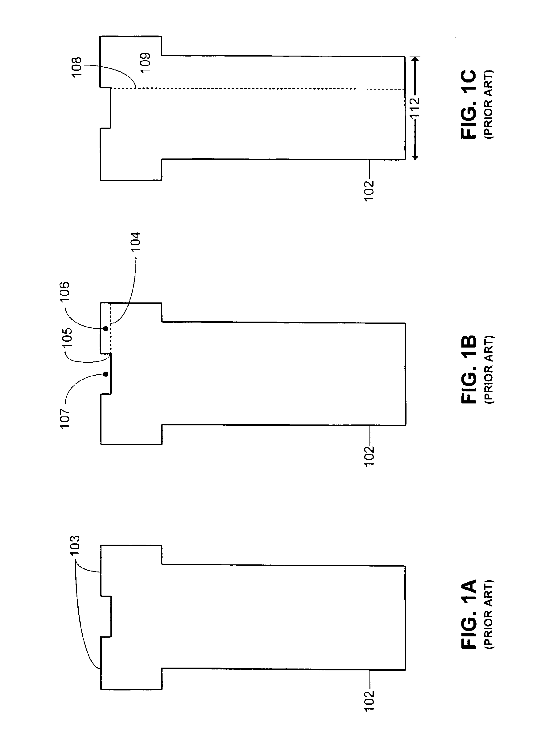
However, this cut is rejected because it creates a “sliver”106, which is too small to be printed easily.
However, slicing the polygon 102 lengthwise in this way fractures critical dimension 112 into multiple rectangles, which can create registration problems during the multiple exposures required to expose the mask blank.
If this aperture is too narrow, the exposure will be less successful than normal.
Method used
View moreImage
Smart ImageViewing Examples

Examples
example
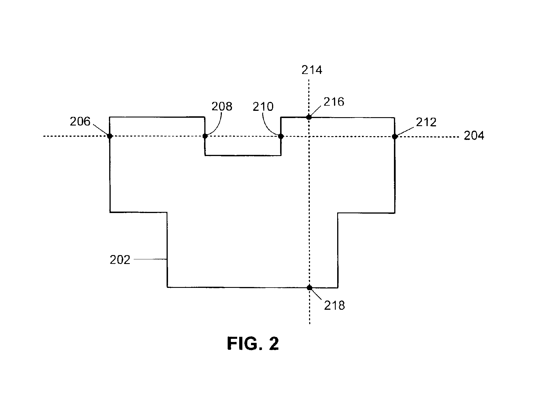
[0047]FIG. 6A illustrates an exemplary fracturing of a layout using an existing technique. In contrast, FIG. 6B illustrates an exemplary fracturing of the same layout using a technique that considers the aspect ratios generated by each slice in accordance with an embodiment of the present invention and makes use of roof cuts. Note that the existing technique fractures some of the wires lengthwise, which can cause critical dimension problems, whereas the new technique does not because it considers aspect ratios. Note also that this technique can be applied to any polygon that is x-convex or y-convex, but not to polygons that are both or neither x-convex and y-convex.
Login to View More PUM
| Property | Measurement | Unit |
|---|---|---|
| aspect ratio | aaaaa | aaaaa |
| aspect ratio | aaaaa | aaaaa |
| aspect ratio | aaaaa | aaaaa |
Abstract
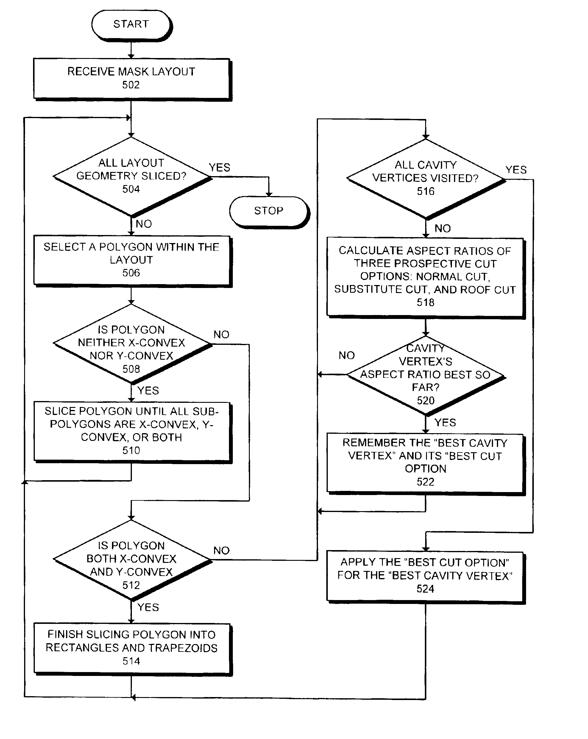
A system for fracturing polygons on masks used in lithography processes for manufacturing an integrated circuit is described. The system fractures polygons that include cavities in either the horizontal edges or the vertical edges by examining the aspect ratio (length / width) of prospective slices made at each vertex of the polygon. After determining the aspect ratio of each prospective slice, the system selects the slice with the lowest aspect ratio and slices the polygon into two sub-polygons. Slicing the polygon in this manner effectively eliminates “slivers” or slices with extreme aspect ratios. This process is continued until each sub-polygon is either a rectangle or a trapezoid that can be printed by electron beam photolithography.
Description
BACKGROUND[0001]1. Field of the Invention[0002]The invention relates to the process of fabricating integrated circuits. More specifically, the invention relates to a method and an apparatus for fracturing polygons on masks used in an optical lithography process for fabricating integrated circuits.[0003]2. Related Art[0004]Recent advances in integrated circuit technology have largely been accomplished by decreasing the feature size of circuit elements on a semiconductor chip. As the feature size of these circuit elements continues to decrease, circuit designers are forced to deal with problems that arise as a consequence of the optical lithography process that is typically used to manufacture integrated circuits. This optical lithography process begins with the formation of a photoresist layer on the surface of a semiconductor wafer. A mask composed of opaque regions, which are generally formed of chrome, and light-transmissive clear regions, which are generally formed of quartz, is ...
Claims
Login to View More Application Information
Patent Timeline
 Patent Type & AuthorityPatents(United States)
IPC IPC(8): G03F9/00G06F17/50G03F1/00G03F1/36
CPCG03F1/36G03F1/144G03F1/68
InventorLUTTRELL, BRUCE
OwnerSYNOPSYS INC