Light-emitting diode

a diode and light-emitting technology, applied in the field of light-emitting diodes, can solve the problems of increasing printing costs, not being widely used, and not being practical with the diode for green and blue, and achieve the effect of increasing the quantity of light and high outpu

Inactive Publication Date: 2005-05-03
FUJIFILM HLDG CORP +1
View PDF5 Cites 3 Cited by
  • Summary
  • Abstract
  • Description
  • Claims
  • Application Information

AI Technical Summary

Benefits of technology

[0012]The present invention has been made in view of the aforementioned circumstances. Accordingly, it is the primary object of the present invention to provide an LED with a stripe waveguide structure that is capable of realizing high output and increasing the quantity of light which can be collected to a microspot, by guiding light more effectively.

Problems solved by technology

However, the former is able to use a semiconductor laser for red, but semiconductor lasers for green and blue have not been put to practical use.
As a result, the latter cannot be widely used for various purposes, and the printing cost increases.
Because of this, the material cost becomes high and consequently the running cost and the printing cost will be increased.
However, for blue and green, it is difficult to obtain semiconductor lasers, and in the solid-state lasers currently in use, cost reduction like a semiconductor laser is difficult due to the number of components and the assembly cost.
Therefore, to constitute a high-definition printer, if the LEDs are employed as light sources to form a spot of a few ten μm in diameter, there is a problem that the light quantity of divergent light which is coupled into the finite aperture of an optical system will become extremely small, and that since an image is formed by a reduction optic system of about ½ to {fraction (1 / 10)}, the lens is moved away from the light source and therefore the coupling efficiency will be further reduced.
However, it has become apparent that in an LED, that does not employ a resonator, it is not optimal to utilize the same design as that of a semiconductor laser.
Particularly, in semiconductor lasers, the reflectance factor at the resonator end plane and the resonance length are important design factors, because they can be the main cause of the efficiency loss of the resonator.
On the other hand, the LED, which has practically no stimulated emission or no stimulated emission at all, is quite different in design from the semiconductor laser, because it does not operate as a resonator, even if it has a similar stripe structure.
Furthermore, since spontaneous emission light is not high in wave-guiding efficiency, the light emitted from the rear end portion of the stripe waveguide region is absorbed in the active layer and therefore it is not effectively emitted from the front facet.

Method used


Image

  • Light-emitting diode
  • Light-emitting diode
  • Light-emitting diode

Examples


first embodiment

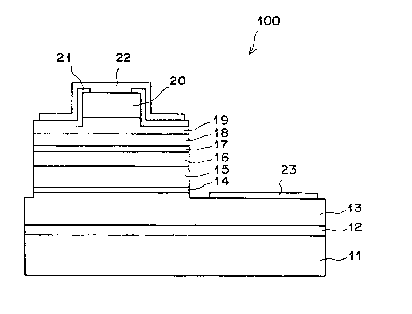
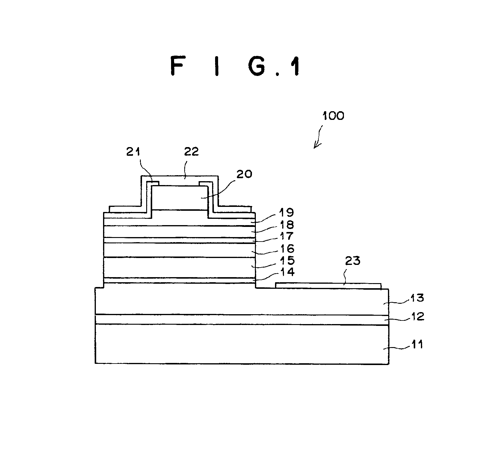
[0026]An InGaN blue LED according to the present invention will hereinafter be described with reference to FIG. 1, along with the fabrication process thereof.

[0027]As shown in FIG. 1, an n-GaN low-temperature buffer layer 12, an n-GaN buffer layer 13 (doped with Si and of a thickness of 5 μm), an n-In0.05Ga0.95N buffer layer 14 (doped with Si and of a thickness of 0.1 μm), an n-Al0.15Ga0.85N clad layer 15 (doped with Si and a thickness of 0.4 μm), an n-GaN optical guide layer 16 (doped with Si and of a thickness of 0.12 μm), an undoped active layer 17, a p-GaN optical guide layer 18 (doped with Mg and of a thickness of 0.12 μm), a p-Al0.15Ga0.85N clad layer 19 (doped with Mg and of a thickness of 0.4 μm), and a p-GaN cap layer 20 (doped with Mg and of a thickness of 0.3 μm), are grown epitaxially upon a sapphire C-plane substrate 11 by metalorganic chemical-vapor deposition (MOCVD). Thereafter, a p-type impurity is activated in an ambient atmosphere of nitrogen gas by heat treatment...

second embodiment

[0035]Next, an InGaN blue LED according to the present invention will be described with reference to FIG. 4, along with the fabrication process.

[0036]The LED of the second embodiment is the same in basic layer structure and fabrication method as the first embodiment. Therefore, the same reference numerals will be applied to the same parts as the first embodiment to avoid redundancy.

[0037]In the LED with a stripe width of 4 μm according to the second embodiment, the thicknesses of an n-GaN guide layer 16 and a p-GaN optical guide layer 18 are both set thicker (1.5 μm). In addition, the ridge process is performed so that a portion of the n-GaN guide layer 16 other than the stripe portion is removed. If the entire optical guide layer is thus formed into a stripe shape, spontaneous emission light is effectively guided to the front facet of the LED and therefore the light-collecting efficiency is enhanced.

[0038]Next, an InGaN blue LED according to a third embodiment of the present invent...

third embodiment

[0039]As shown in FIG. 5, in the LED of the third embodiment, the 6H—Si substrate 31 with n-type conductivity is employed as the substrate. For this reason, an n-type electrode 23 is formed on the bottom surface of the 6H—Si substrate 31.

[0040]In the three embodiments described above, the LEDs have light emission wavelengths in a blue region. However, the present invention is also applicable to LEDs having light emission wavelengths in a region of green (492 nm or greater), a region of violet (450 nm or less), or an ultraviolet region of further shorter wavelengths. For ultraviolet, for instance, the present invention is also applicable to an LED which has a GaN or AlGaN active layer, an AlGaN optical guide layer, and an AlGaN clad layer. An AlGaN / GaN superlattice, etc., can be employed as the clad layer.

[0041]Furthermore, in the aforementioned embodiments, the ridge-shaped stripe structure with an insulating film has been described as the device structure. However, the present inve...


PUM


Abstract

An n-GaN low-temperature buffer layer, an n-GaN buffer layer, an n-In0.05Ga0.95N buffer layer, an n-Al0.15Ga0.85N clad layer, an n-GaN optical guide layer, an undoped active layer, a p-GaN optical guide layer, a p-Al0.15Ga0.85N clad layer, and a p-GaN cap layer, are grown on a sapphire substrate. Then, an epitaxial layer other than a light-emitting region is etched until the n-GaN buffer layer is exposed. Next, in a similar process, etching is performed up to anywhere within the p-Al0.15Ga0.85N clad layer so that a 4-μm-wide stripe region in the form of a ridge remains. The length from the light-emitting facet to the opposite facet is between 30 and 250 μm.

Description

BACKGROUND OF THE INVENTION[0001]1. Field of the Invention[0002]The present invention relates to light-emitting diodes (LEDs) having a stripe waveguide structure.[0003]2. Description of the Related Art[0004]As a conventional printing system for a high definition photograph, a digital printer (“Frontier”) equipped with an exposure system has been produced by the present applicant. The exposure system is used to expose a regular photosensitive material by employing a semiconductor laser as a red light source and also employing solid-state excitation lasers (utilizing second harmonic generation (SHG)) as blue and green light sources. In addition, there has been produced a relatively inexpensive exposure system (“Pictography”) for exposing a photosensitive material that generates the colors to cyan, magenta, and yellow, by the use of a semiconductor laser light with two infrared wavelengths and a red wavelength. These exposure systems can perform high-speed light-beam scanning by employ...

Claims


Application Information

Patent Timeline
Patent Type & Authority Patents(United States)
IPC IPC(8): H01L33/00H01L33/06H01L33/10H01L33/12H01L33/32H01L33/44H01L33/46
CPCH01L33/46H01L33/20H01L33/32
Inventor HAYAKAWA, TOSHIRO
Owner FUJIFILM HLDG CORP
Why Eureka
Try Eureka