In-situ film thickness measurement using spectral interference at grazing incidence

a grazing incidence and in-situ film technology, applied in the field of wafer processing, can solve the problems of non-optimal or undesirable properties of layers, inability to provide information regarding periodic process quality assessment methods, and substantial waste, so as to improve the signal-to-noise ratio and reduce the cost

Inactive Publication Date: 2005-05-03
APPLIED MATERIALS INC
View PDF9 Cites 26 Cited by
  • Summary
  • Abstract
  • Description
  • Claims
  • Application Information

AI Technical Summary

Benefits of technology

[0010]An additional embodiment of the method of the present invention uses an interference filter to confine the spectral composition of the plasma emissions to an emission at a narrow wavelength interval and a

Problems solved by technology

This process is time consuming and potentially results in wafers that do not meet the production specifications, as process drift may result in variable deposition rates.
This method can result in a substantial waste, since deviations from desired process parameters, and thus the production of film layers having non-optimal or undesirable properties, are only detected after a whole group of wafers has been processed.
An additional limitation of the current test wafer thickness monitoring is that it is only capable of disclosing whether a particular film layer pos

Method used


Image

  • In-situ film thickness measurement using spectral interference at grazing incidence
  • In-situ film thickness measurement using spectral interference at grazing incidence
  • In-situ film thickness measurement using spectral interference at grazing incidence

Examples


Embodiment Construction

I. An Exemplary Plasma Enhanced Chemical Vapor Deposition (PECVD) Chamber Configured to Practice the Present Invention

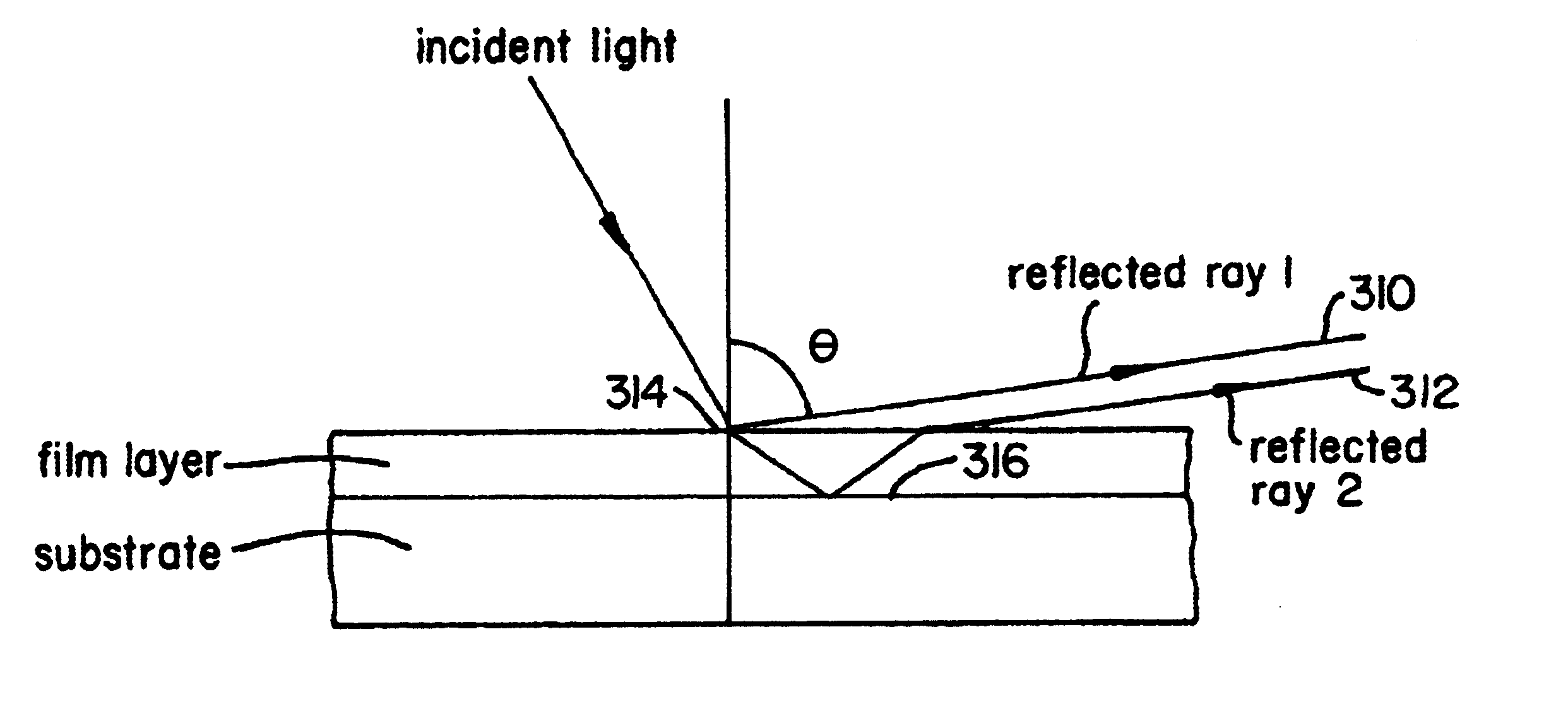
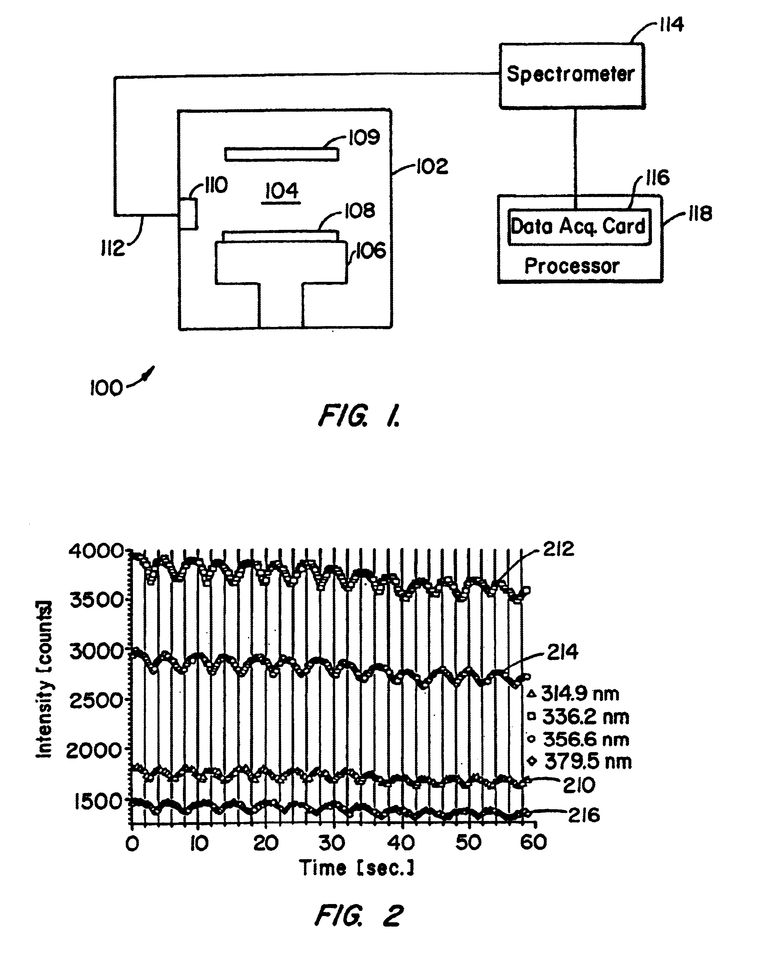
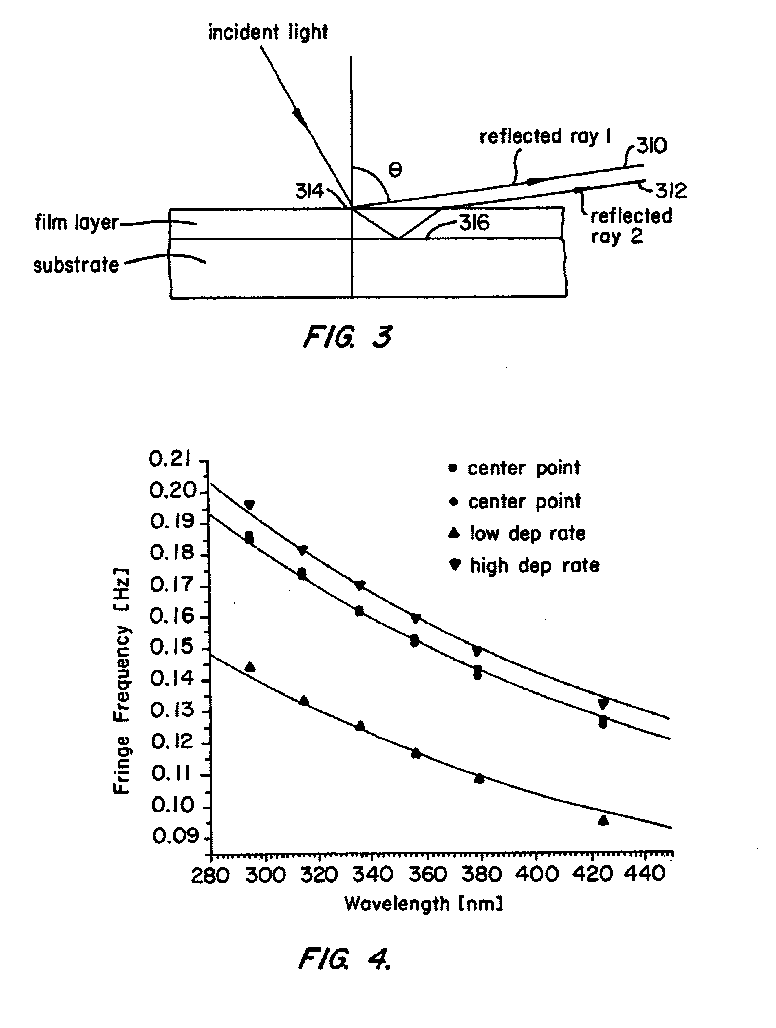
[0022]The method of the present invention can be used with any standard plasma deposition chamber that includes a side-view window or side-viewport through which plasma emissions reflected off the surface of the wafer can be directed to a light detection and analysis device. In one embodiment, the light detection device can be a spectrometer. FIG. 1 is a simplified cross-sectional view of an exemplary PECVD chamber 100 configured to practice the method of the present invention. As shown in FIG. 1, PECVD chamber 100 includes a housing 102 that surrounds a substrate processing region 104. During a deposition process a substrate 108 is supported on a pedestal 106 and exposed to a plasma formed in region 104. The plasma generates electromagnetic radiation that includes emissions having wavelengths in the optical spectrum (i.e., from 200 nm to 900 nm). A portion of these ...


PUM


Abstract

A method and system using spectral interference of light from plasma emissions collected at near grazing incidence to in-situ monitor and control the film thickness of a non-opaque film. Embodiments of this invention are particularly useful to all substrate processing chambers equipped to form an in-situ plasma within the chamber and which are used to deposit or etch non-opaque films. One embodiment of the method of the present invention forms a plasma within a substrate processing chamber to deposit a non-opaque film on a wafer substrate within the chamber. During the plasma deposition process, a plurality of wavelengths of radiation including those reflected from the top and bottom layer of the film being deposited upon a wafer surface are collected through an existing viewport, and conveyed to a spectrometer for measurements via an optical fiber attached near this viewport. These measurements are analyzed to determine the film's thickness. An alternate embodiment of the method of the present invention uses an interference filter to confine the spectral composition of the plasma emissions to an emission at a narrow wavelength interval and a photodiode to detect the intensity of the emission.

Description

BACKGROUND OF THE INVENTION[0001]The present invention is related to wafer processing and in particular to a method of monitoring a deposition or an etch process. More specifically, the present invention relates to a method of measuring the thickness of a film layer being deposited by a plasma enhanced chemical vapor deposition process (PECVD) or etched by a plasma etch process. The present invention may be used to measure the deposition or etch rate and film thickness of a variety of optically transparent films.[0002]To provide repeatable device performance, the thickness of film layers must be maintained within specified tolerances. One methodology for determining the thickness of a film layer being deposited is to time the deposition and factor the time period with a theoretical rate to approximate the film thickness. To establish the actual deposition rate in a chamber, a semiconductor manufacturer processes and subsequently measures a film deposited on a few test wafers. The fi...

Claims


Application Information

Patent Timeline
IPC IPC(8): G01B11/06G01N21/88G01N21/95G01N21/84H01L21/66
CPCG01B11/0675G01N21/8422H01L22/26G01N21/9501H01L22/12
Inventor GOEBEL, ANDREASSARFATY, MOSHERAOUX, SEBASTIEN
Owner APPLIED MATERIALS INC
Why Eureka
Try Eureka