High frequency module board device

a module board and high frequency technology, applied in the direction of high frequency circuit adaptation, electric apparatus casing/cabinet/drawer, direct conversion system, etc., can solve the problem of increasing the forming step to increase the manufacture cost, the transmitting and receiving circuit cannot obtain adequate characteristics, etc., to achieve the effect of parasitic capacity and capacitance characteristics respectively improving

Inactive Publication Date: 2005-05-03
SONY CORP
View PDF6 Cites 42 Cited by
  • Summary
  • Abstract
  • Description
  • Claims
  • Application Information

AI Technical Summary

Benefits of technology

[0034]This high frequency module board device has the first capacitance formed in such a way that the insulating layer is interposed between the upper electrode part formed in the upper wiring layer and the lower electrode part formed in the lower wiring layer just above the area in which the wiring is not formed in the wiring layer of the base board. Further, the high frequency module board device has the second capacitance formed in such a way that the electrode part formed on the first wiring layer counted from the build-up surface of the base board is interconnected to the upper electrode part to interpose the insulating layer between the lower electrode part and the electrode part. In this high frequency module board device, the capacitance can be adequately separated from the wiring layers of the base board. Parasitic capacities generated by the wiring layers of the base board are respectively reduced relative to the capacitance, so that the characteristics of the capacitance are respectively improved.

Problems solved by technology

The conventional high frequency transmitting and receiving circuits of both the super-heterodyne system and the direct conversion system, as mentioned above, cannot obtain adequate characteristics as the transmitting and receiving circuits, in addition to the miniaturization and light-weight of the communication terminal equipment.
In the high frequency module board 120 constructed as described above, a forming step of the inductance 121 is complicated, so that the forming steps are increased to increase a manufacture cost.
In the conventional high frequency module board device, the electrical interference of the Si substrate provided between a circuit part of an analog circuit and a base-band circuit part of a digital circuit constitutes a serious problem.
However, this substrate undesirably constitutes a factor of interference upon realizing the good high frequency characteristics of the respective passive elements.
Further, since the wiring layers are formed in multi-layers, a manufacture cost is increased.

Method used


Image

  • High frequency module board device
  • High frequency module board device
  • High frequency module board device

Examples


Embodiment Construction

[0054]Now, embodiments of a high frequency module board device according to the present invention will be described in detail by referring to the drawings.

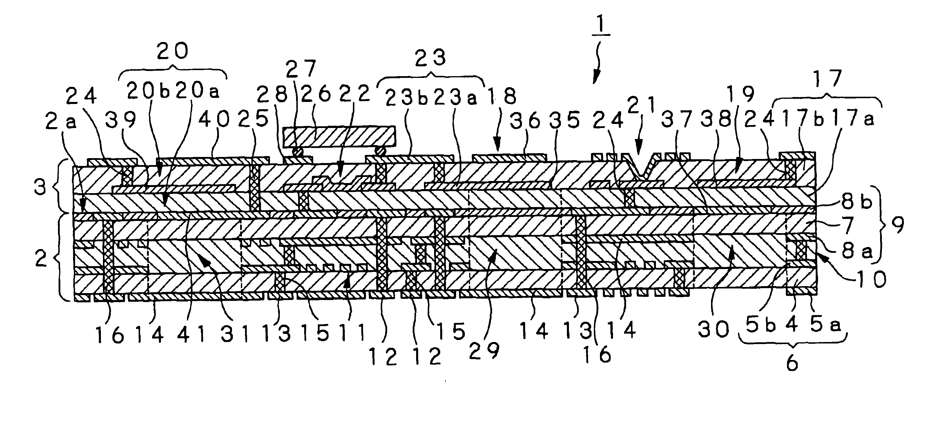
[0055]A high frequency module board device 1 according to the present invention shown in FIG. 7 has a package form for realizing a high density mounting structure to a mother board or an interposer board (intermediate board) and this device itself serves as one functional parts.

[0056]The high frequency module board device 1 according to the present invention comprises a base board 2, the uppermost layer of which is formed in a highly accurate flat surface as a build-up surface 2a, and a high frequency circuit part 3 built up thereon.

[0057]The base board 2 is a what is called a printed-wiring board. The base board 2 has a structure having a first wiring board 6 in which first and second wiring layers 5a and 5b are patterned on both the surfaces of a first core board 4 as a dielectric insulating layer. Further, the base board 2 has ...


PUM

PropertyMeasurementUnit
dielectric constantaaaaaaaaaa
frequencyaaaaaaaaaa

Abstract

The present invention relates to a high frequency module board device having a high frequency transmitting and receiving circuit for modulating and demodulating a high frequency signal. The high frequency module board device comprises a base board (2) whose main surface is formed as a build-up surface (2a) and a high frequency circuit part (3) formed on the build-up surface of the base board (2) and having passive elements formed. The base board (2) has an area (29) in which wiring is not formed in a lower layer from a fourth wiring layer (8b). The high frequency circuit part (3) has an upper electrode part (36) and a lower electrode part (35) in positions corresponding to the area (29) in which the wiring is not formed. Thus, since a capacitance (18) is provided just above the area (29) in which the wiring is not formed, a parasitic capacity that the capacitance (18) receives from ground patterns (14) is reduced. Accordingly, the characteristics of the capacitance (18) can be improved.

Description

TECHNICAL FIELD[0001]The present invention relates to a high frequency module board device comprising a base board and a high frequency circuit part.BACKGROUND ART[0002]Various kinds of information such as music, audio data, images or the like can be readily treated by compact information processors such as personal computers or mobile computers with the digitization of data. The band of these information has been compressed by an audio codec technique or an image codec technique. Thus, an environment in which the information is easily and efficiently distributed to various kinds of communication terminal equipment by a digital communication or a digital broadcasting has been arranged. For instance, audio data and video data (refer them to as AV data, hereinafter) may be received outdoors by portable telephones.[0003]The transmitting and receiving system of data or the like has been conveniently utilized in small areas as well as in homes in various ways by forming preferable networ...

Claims


Application Information

Patent Timeline
Patent Type & Authority Patents(United States)
IPC IPC(8): H01L23/58H01L23/66H05K1/16H05K1/00H05K1/02H05K3/46H01F17/00H01L23/12H01L23/498H01P1/00H01P3/08
CPCH01L23/49822H01L23/66H05K1/162H01L23/49805H01F17/0006H01L2224/16235H01L2224/16H01L2224/48091H01L2924/01078H01L2924/19011H01L2924/19105H01L2924/19107H01L2924/30107H01L2924/3025H05K1/0224H05K1/024H05K1/0298H05K3/4688H05K2201/09672H01L2224/16225H01L2924/10253H01L2924/01087H01L24/48H01L2924/00014H01L2924/00H01L2924/12042H01L2224/05599H01L2224/45099H01L2224/85399H01L2924/14H01L2224/45015H01L2924/207H01L25/00
Inventor OGINO, TATSUYAOKUBORA, AKIHIKOHIRABAYASHI, TAKAYUKIKOSEMURA, TAKAHIKOHAYASHI, KUNIYUKI
Owner SONY CORP
Why Eureka
Try Eureka