Material for forming exposure light-blocking film, multilayer interconnection structure and manufacturing method thereof, and semiconductor device

a technology of exposure light and film, which is applied in the direction of photomechanical equipment, instruments, transportation and packaging, etc., can solve the problems of increasing the interconnection resistance (r), the interconnection delay, and the inability to achieve a speedup, so as to reduce the parasitic capacity between the interconnection and the effect of reducing the interconnection resistan

Inactive Publication Date: 2010-06-01
FUJITSU LTD
View PDF23 Cites 4 Cited by
  • Summary
  • Abstract
  • Description
  • Claims
  • Application Information

AI Technical Summary

Benefits of technology

[0015]The multilayer interconnection structure of the present invention includes at least an exposure light-blocking film, a porous insulating film, and an interconnection layer, and the exposure light-blocking film is formed by use of the material of the present invention for forming an exposure light-blocking film. For this reason, the exposure light-blocking film has excellent exposure light (e.g., ultraviolet light) absorptivity and exhibits an ultraviolet light blocking function. For example, when the exposure light-blocking film is formed on the porous insulating film, the exposure light (e.g., ultraviolet light) is prevented from reaching the porous insulating film. Thus, when a porous insulating film that has been deposited above the exposure light-blocking film is to be irradiated with exposure light (ultraviolet light) for curing, it is possible to efficiently prevent ultraviolet light from reaching other porous insulating films provided below the porous insulating film (or exposure target), thereby reducing damages to them caused as a result of repeated curing operations and preventing the reduction in the amounts of these porous insulating films. Moreover, in the case of electron beams, damages to transistors in the lowermost layer can be reduced with this configuration. The porous insulating films have low permittivity and therefore, it is possible to reduce parasitic capacities and to achieve high-speed signal propagation. For these reasons, the multilayer interconnection structure of the present invention is particularly suitable for highly-integrated semiconductor integrated circuits such as ICs and LSIs, which require high response speed.
[0016]Conventionally, it has been known that increased parasitic capacities in insulating films cause a reduction in the signal propagation speed. In a semiconductor device with an interconnection pitch of as large as 1 μm or more, however, interconnection delay has less effect on the whole of the semiconductor device. In recent years, interconnection width and interconnection pitch are becoming narrower and narrower along with increased packaging densities of semiconductor integrated circuits and with the advent of multilayer interconnection structures; in particular, the problem of increased interconnection resistance and increased parasitic capacities is prominent in semiconductor devices with an interconnection pitch of as small as 1 μm or less. Because both the interconnection resistance and parasitic capacities between interconnections—major factors that control the performance of devices such as semiconductor integrated circuits—determine the signal propagation speed in a multilayer interconnection structure of the semiconductor integrated circuits, the increased interconnection resistance and increased parasitic capacities are a big problem that needs to be overcome as the cause that reduces the signal propagation speed. For an increased signal propagation speed, it is necessary to reduce both the interconnection resistance and the parasitic capacities between interconnections (or the permittivities of the insulating films). Although the parasitic capacities between interconnections can be reduced by making the interconnections thin to reduce their cross-section areas, thin interconnections cause an increase in the interconnection resistance. This means that achieving an increased signal propagation speed is a trade-off between reduced parasitic capacities between interconnections and reduced interconnection resistance. At present, coating-type porous insulating films have been proposed as low permittivity-insulating films. Such insulating films, however, are poor in their mechanical strength because they are porous, thus requiring reinforcement. Examples of the methods for increasing the mechanical strength of such insulating films includes a method for curing an insulating film by applying exposure light (e.g., ultraviolet light) to it. The use of the exposure light-blocking film in such a method can reduce both the parasitic capacities between interconnections and interconnection resistance, making it possible to increase the signal propagation speed.
[0017]The method of the present invention for forming a multilayer interconnection structure is a method for forming the multilayer interconnection structure of the present invention, the method including at least an exposure light-blocking film formation step, a porous insulating film formation step, a curing step, and an interconnection formation step. In the exposure light-blocking film formation step an exposure light-blocking film is formed on a work surface by use of the material of the present invention for forming an exposure light-blocking film. In the porous insulating film formation step a porous insulating film is formed on the exposure light-blocking film. In the curing step the porous insulating film is cured by irradiation with exposure light. In the interconnection formation step an interconnection is formed. By repeating these steps, a multilayer interconnection structure is efficiently formed. The method for manufacturing a multilayer interconnection structure is particularly suitable for the manufacturing of the multilayer interconnection of the present invention.
[0018]The semiconductor device of the present invention includes at least the multilayer interconnection structure of the present invention. Since this semiconductor device includes the multilayer interconnection structure of the present invention, the parasitic capacities between interconnections and interconnection resistance can be reduced. For this reason, the semiconductor device of the present invention is particularly suitable for high-speed, highly-reliable flash memories, DRAMs, MOS transistors and so forth.

Problems solved by technology

Against this background, the interval between adjacent interconnections, or interconnection interval, has become smaller and smaller, leading to a problem of interconnection delay due to an increased capacity between interconnections.
The reduction of the capacity (C) can be achieved by reducing the interconnection thickness and the electrode area, though, reducing the interconnection thickness causes an increase in the interconnection resistance (R), making it impossible to achieve a speedup.
In addition, the SiOF film, an insulating film explored as a candidate for a low-permittivity CVD film, has a permittivity of as small as 3.3 to 3.5, but highly hygroscopic; therefore, the SiOF film has a problem that the permittivity increases with time.
For this reason, increasing the porosity for reduced permittivity leads to a problem of increased permittivity and / or reduced film strength, caused due to moisture absorption.
However, ultraviolet light and plasmas unfavorably reach other films provided below the insulating film which is to be irradiated with them (or an exposure target).
Moreover, there is a concern about the use of electron beams because their exposure energy is particularly high enough to undesirably damage transistors present in the lowermost layer.

Method used


Image

  • Material for forming exposure light-blocking film, multilayer interconnection structure and manufacturing method thereof, and semiconductor device
  • Material for forming exposure light-blocking film, multilayer interconnection structure and manufacturing method thereof, and semiconductor device
  • Material for forming exposure light-blocking film, multilayer interconnection structure and manufacturing method thereof, and semiconductor device

Examples


example 1

—Preparation of Material for Forming an Exposure Light-Blocking Film—

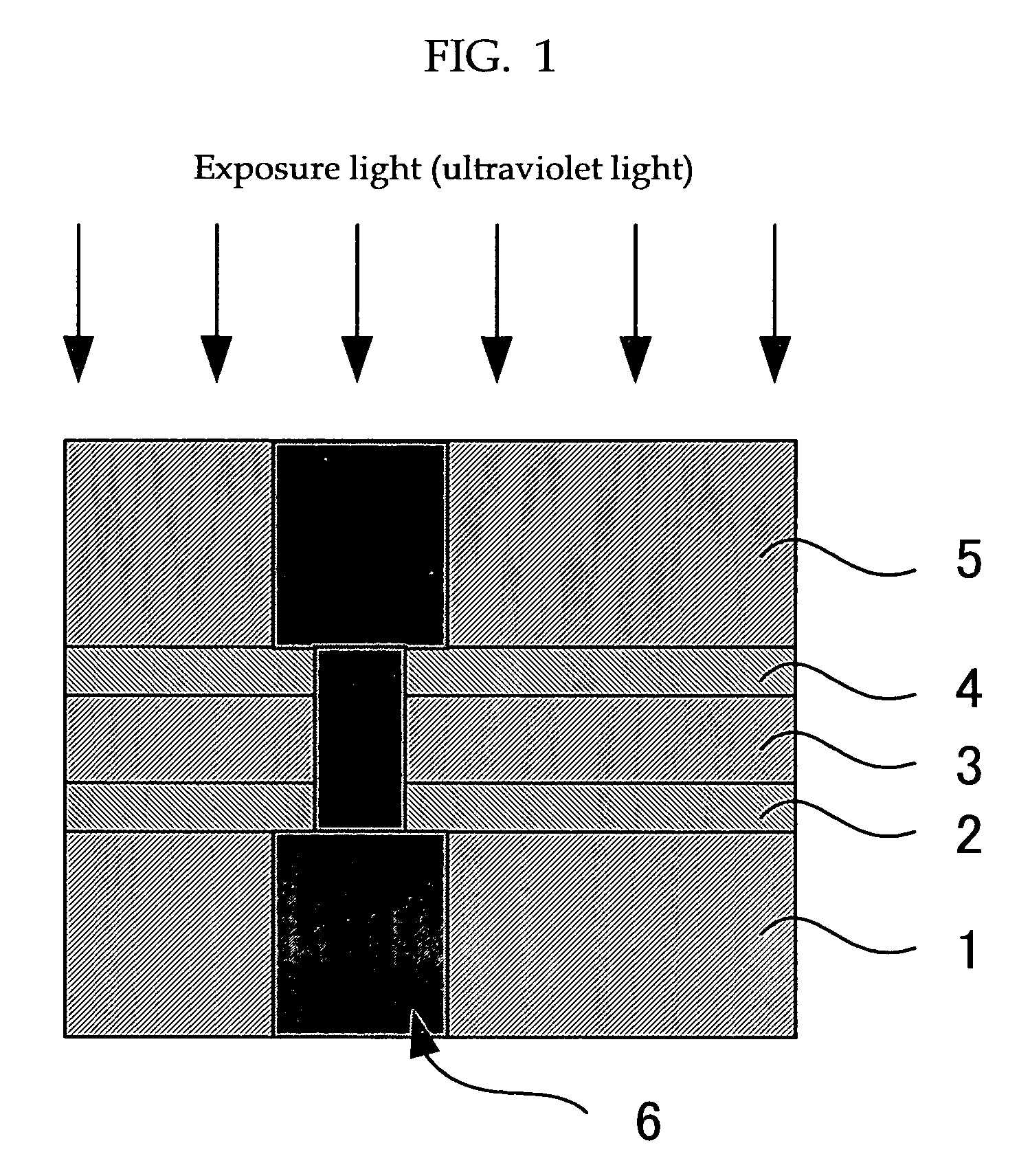
[0158]At least one of R1 and R2 in a polycarbosilane expressed by the structural formula (1) was halogenated and reacted with Grignard reagent containing a vinyl group—a substitutent capable of absorbing ultraviolet light. In this way a material for forming an exposure light-blocking film, which contains a polycarbosilane expressed by the structural formula (1) where at least one of R1 and R2 is replaced by a vinyl group was prepared.

—Manufacturing of the Multilayer Interconnection Structure and Semiconductor Device—

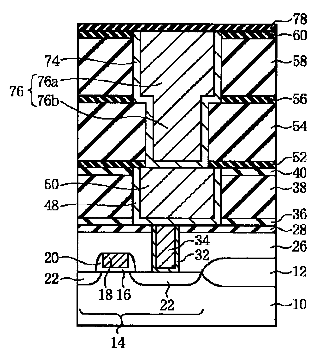
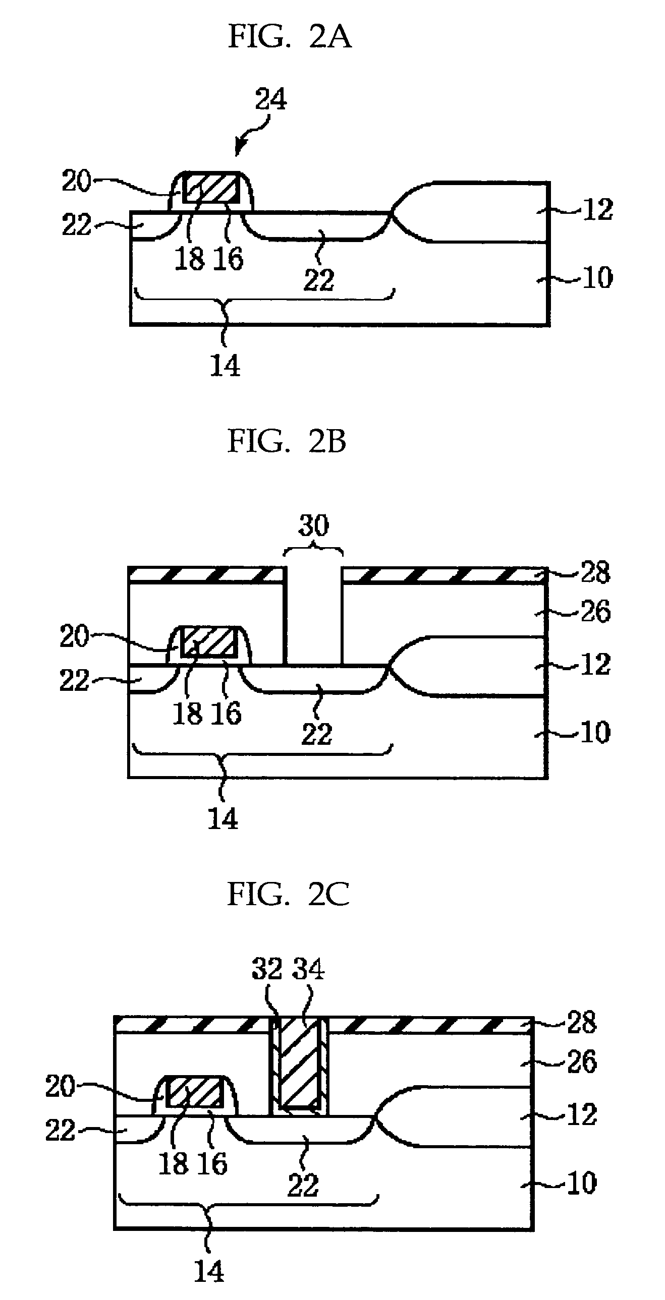
[0159]Both the multilayer interconnection structure and semiconductor device of the present invention were manufactured in the manner described below. At first, as shown in FIG. 2A, an element separation film 12 was formed on a semiconductor substrate 10 with a LOCOS (Local Oxidation of Silicon) method. The element separation film 12 defined an element region 14. Note that a silicon substrate was adopte...

examples 2 to 12

[0185]Semiconductor devices were manufactured in a manner similar to that described in Example 1 except that the material for forming an exposure light-blocking film was changed to those shown in Table 1 and an exposure light-blocking film was formed as the first interlayer insulating film. In addition, the effective permittivities of the resultant semiconductor devices, semiconductor device manufacturing yields, and the reduction in the amounts of the porous insulating films provided below the exposure light-blocking film were measured in a manner similar to that described in Example 1. The results are also shown in Table 1.

[0186]Note in Examples 2, 4, 6, 8, 10 and 12 that as the third interlayer insulating film a SiC film capable of admitting ultraviolet light was formed on the porous insulating film that serves as the second interlayer insulating film, and that ultraviolet light was applied on the porous insulating film for curing through the SiC film.


PUM

PropertyMeasurementUnit
thicknessaaaaaaaaaa
thicknessaaaaaaaaaa
thicknessaaaaaaaaaa

Abstract

To provide a material for forming an exposure light-blocking film which includes at least one of a silicon compound expressed by the following structural formula (1) and a silicon compound expressed by the following structural formula (2), wherein at least one of R1 and R2 is replaced by a substituent capable of absorbing exposure light.(where R1 and R2 may be the same or different, and each represents any one of a hydrogen atom, alkyl group, alkenyl group, cycloalkyl group and aryl group which are optionally substituted, and n is an integer of 2 or greater)(where R1, R2 and R3 may be the same or different, at least one of R1, R2 and R3 represents a hydrogen atom and the others represent any one of an alkyl group, alkenyl group, cycloalkyl group and aryl group which are optionally substituted, and n is an integer of 2 or greater)

Description

CROSS-REFERENCE TO RELATED APPLICATIONS[0001]This application is based upon and claims the benefits of the priority from the prior Japanese Patent Application No. 2006-037025 filed on Feb. 14, 2006, the entire contents of which are incorporated herein by reference.BACKGROUND OF THE INVENTION[0002]1. Field of the Invention[0003]The present invention relates to an exposure light-blocking film that is suitable for a multilayer interconnection structure in a semiconductor integrated circuit and can efficiently block exposure light (e.g., ultraviolet light) applied to a porous insulating film; to a material for forming an exposure light-blocking film, which is suitably used for the formation of the exposure light-blocking film; to a multilayer interconnection structure provided with the exposure light-blocking film and a manufacturing method thereof; and to a semiconductor device provided with the multilayer interconnection structure and a manufacturing method thereof.[0004]2. Descriptio...

Claims


Application Information

Patent Timeline
Patent Type & Authority Patents(United States)
IPC IPC(8): C08L83/04C08G77/60H01L21/312H01L21/314H01L21/768H01L23/522
CPCC08L83/16H01L21/02164H01L21/022H01L21/02203H01L21/02211H01L21/02282H01L21/3105H01L21/3121H01L21/3125H01L21/31695H01L21/3185H01L21/76829H01L2924/0002H01L21/76807H01L2924/00Y10T428/31663H01L21/3205
Inventor OZAKI, SHIROUNAKATA, YOSHIHIRO
Owner FUJITSU LTD
Why Eureka
Try Eureka