Method for forming a thin film transistor of an organic light emitting display

a thin film transistor and organic light-emitting display technology, applied in the direction of transistors, semiconductor devices, electrical equipment, etc., can solve the problems of low electron mobility of amorphous silicon layer, inability to meet the large-sized and high-dpi display, and uncertain gate threshold voltage of tft, so as to reduce the threshold voltage shifting of the gate, prolong the life of the oled, and improve the performance quality of the oled

Inactive Publication Date: 2005-05-10
AU OPTRONICS CORP
View PDF4 Cites 37 Cited by
  • Summary
  • Abstract
  • Description
  • Claims
  • Application Information

AI Technical Summary

Benefits of technology

[0017]It is an advantage of the present invention that the method comprises forming a microcrystalline silicon layer on the gate insulating layer, which results in reduced threshold voltage shifting of the gate. Therefore, the performance quality of the OLED can be improved, and t...

Problems solved by technology

Since the light-emitting time of each pixel is restricted by the scanning frequency and the numbers of scan lines, the passive matrix method is not suitable for large-sized and high dots-per-inch (dpi) displays with a high amount of scan lines.
However, according to the prior art, the amorphous silicon layer is composed of silicon molecules that are not crystallized, so that the amorphous silicon layer has low electron mobility.
Furthermore, the threshold voltage of the gate of a TFT with amorphous silicon material will shift depending on the fabrication process, which will result in each TFT having an uncertain gate threshold vol...

Method used


Image

  • Method for forming a thin film transistor of an organic light emitting display
  • Method for forming a thin film transistor of an organic light emitting display
  • Method for forming a thin film transistor of an organic light emitting display

Examples


second embodiment

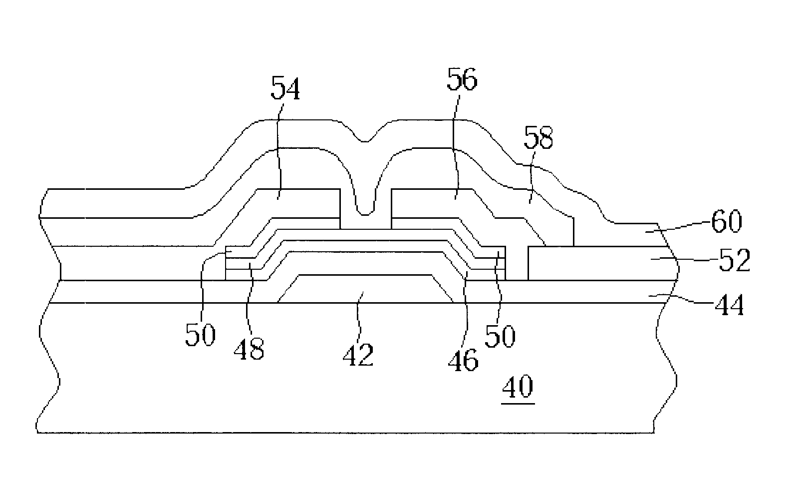
[0026]In the present invention method, a surface treatment is performed after the gate insulating layer 44 is deposited. Therefore, the microcrystalline silicon layer 46 is deposited after the gate insulating layer 44 is treated. This is because the microcrystalline silicon layer 46 will be formed favorably if the interface between the gate insulating layer 44 and the microcrystalline silicon layer 46 contains more oxygen-containing molecules. In this embodiment, a nitrous oxide (N2O) plasma treatment is performed, which results in the gate insulating layer 44 having stronger oxygen bonding with the subsequently formed microcrystalline silicon layer 46 and a stable interface of the gate insulating layer 44 and the microcrystalline silicon layer 46. In addition, the surface treatment process can be an oxygen-containing plasma treatment that also provides stronger oxygen bonding between the gate insulating layer 44 and the microcrystalline silicon layer 46. The oxygen-containing gas o...

third embodiment

[0027]According to the present invention, the gate insulating layer 44 and the microcrystalline silicon layer 46 are formed by an interrupted deposition. For example, after performing a PECVD process to form the gate insulating layer 44, the substrate 40 is moved out of the reaction chamber, and moved into the original reaction chamber or a different reaction chamber to perform the deposition of the microcrystalline silicon layer 46. According to these processes of forming the microcrystalline silicon layer 46, the TFT is given better stability to effectively reduce the shifting influence of the threshold voltage of the gate of a TFT.

[0028]In contrast to the prior art, the present invention method of forming a TFT of an OLED uses a hydrogenated amorphous silicon layer (α-Si:H layer) and a simple low-cost process to form a microcrystalline silicon layer between the gate insulating layer and the amorphous silicon layer. The crystallization ability of the microcrystalline silicon layer...


PUM


Abstract

A method for forming a thin film transistor of an organic light emitting display includes depositing a first metal layer on a substrate, performing a photo-etching-process (PEP) to form a gate of the TFT on the substrate, forming a gate insulating layer, a microcrystalline silicon layer, an amorphous silicon layer, and a doped n+ layer sequentially, and then performing a second PEP to remove a portion of the doped n+ layer, the amorphous silicon layer, and the microcrystalline silicon layer. The method further includes forming a second metal layer, performing a third PEP to form a source and a drain on the substrate and to simultaneously remove a portion of the doped n+ layer to expose the amorphous silicon layer, and finally, forming a passivation layer on the substrate.

Description

BACKGROUND OF INVENTION[0001]1. Field of the Invention[0002]The invention relates to a method for forming a thin film transistor (TFT) of an organic light-emitting display (OLED), and more particularly, to a method for forming a TFT that can solve the problem of threshold voltage shifting of the gate of a TFT.[0003]2. Description of the Prior Art[0004]Since the progress of science and technology has led to small, effective, and portable intelligent information products, display devices have played an important role in modern society. In recent years, display devices have undergone great improvements in the areas of high performance quality, larger size, and lower cost. Among the various display devices in the display market, OLEDsare poised replace liquid crystal displays (LCD) and cathode ray tube (CRT) displays, as they have advantages of simpler structures, self-emitting design, excellent operating temperature, high definition, high contrast, and a wide viewing angle. OLEDs can b...

Claims


Application Information

Patent Timeline
IPC IPC(8): H01L21/00H01L29/66H01L29/786H01L33/00H01L21/336H01L27/32
CPCH01L29/78678H01L29/78669H01L29/66765H01L27/3262H10K59/1213
Inventor LIN, HAN-TULAI, HAN-CHUNG
Owner AU OPTRONICS CORP
Why Eureka
Try Eureka