Integrally formed bake plate unit for use in wafer fabrication system

a wafer fabrication system and integrated technology, applied in the field of bake plate units, can solve the problems of increasing the difficulty of ultraviolet reflectivity, and increasing the difficulty of design goal, and achieve the effect of rapid temperature set-point changes

Inactive Publication Date: 2005-05-10
ASML HLDG NV
View PDF9 Cites 5 Cited by
  • Summary
  • Abstract
  • Description
  • Claims
  • Application Information

AI Technical Summary

Benefits of technology

[0014]The present invention provides an integrally formed bake plate by etching a desired heater element pattern into the lower surface of a machined preferably copper plate, whose upper surface will contact and heat a wafer. A pattern is formed in the lower plate surface defining grooves or channel regions where a heating element structure will be located. Through holes for lift pins are machined, and plate surfaces are coated, preferably with electroplated nickel and CVD diamond-like film to preven

Problems solved by technology

At modern photolithography seeks to define smaller and smaller feature size using shorter wavelength light, ultraviolet reflectivity becomes a greater problem, and thus the use of anti-reflection layer(s).
The challenge in designing a PEB bake plate is to achieve high uniformity in the ability to achieve and maintain within specification a desired and reproducible PEB temperature over a given period of time.
The design goal is made difficult by the fact the spin coater 30 typically can accommodate many different types of photoresists, each requiring a different PEB bake plate temperature and time regime.
Achieving good thermal uniformity across a PEB bake plate that is perhaps 13″ (33 cm) in diameter has been a difficult challenge in the prior art.
Although thermal paste or adhesive (not shown) is used within cavities 170 to help bond with the heater wire, it is difficult to maintain a consistent thermal interfa

Method used


Image

  • Integrally formed bake plate unit for use in wafer fabrication system
  • Integrally formed bake plate unit for use in wafer fabrication system
  • Integrally formed bake plate unit for use in wafer fabrication system

Examples


Embodiment Construction

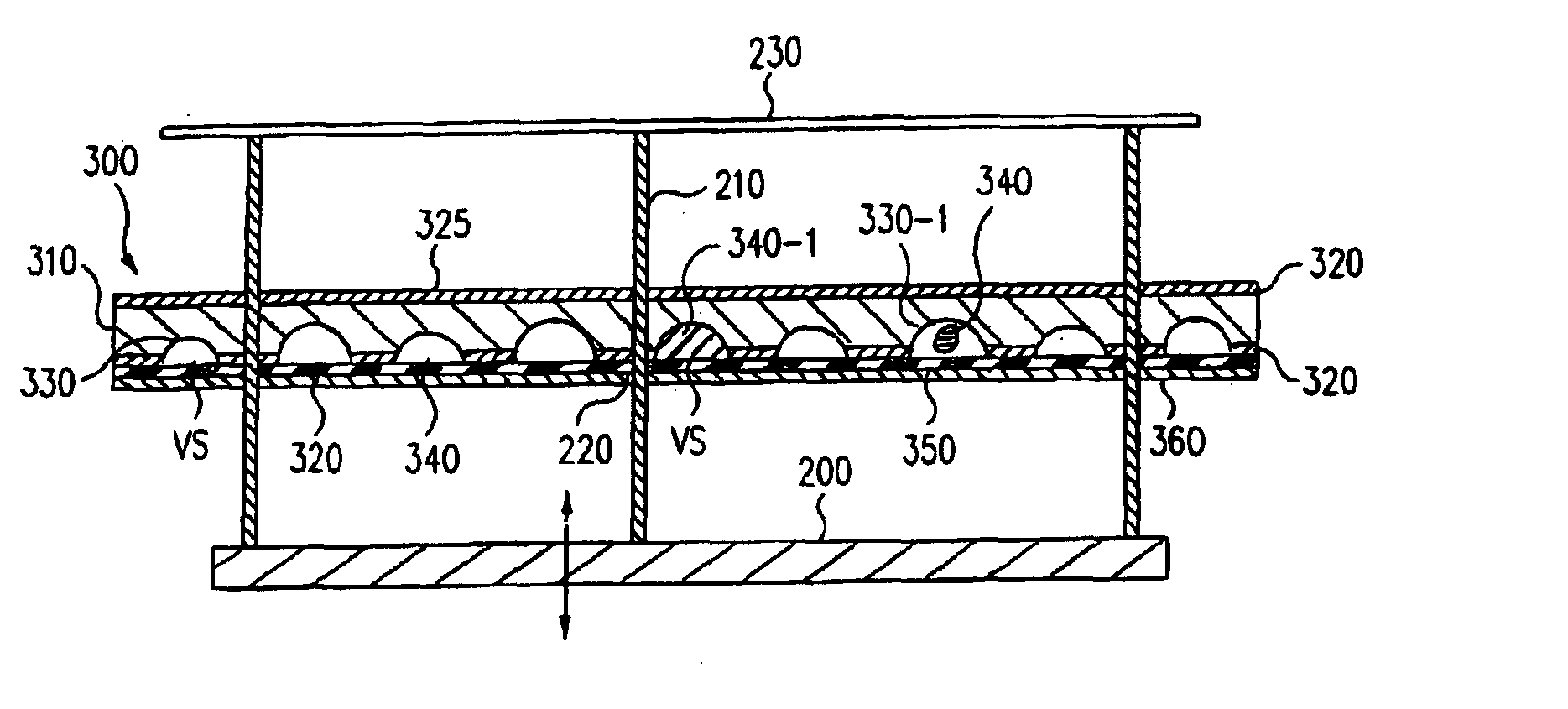
[0022]FIG. 3 depicts an integrally fabricated bake plate 300, according to the present invention. Reference numerals repeated from FIGS. 2A and 2B may be understood to represent similar elements. Thus, element 230 in FIG. 3 is the wafer to be heated when lift pins 210 are lowered vertically by a robotic mechanism 200. FIG. 4 depicts an openable chamber 370 in which a bake plate 300, according to the present invention is situated. FIG. 5 depicts major steps involved in fabricating a bake plate, according to the present invention.

[0023]In FIG. 3 and at method step 400 in FIG. 5, the plate disk 310 is formed to specification, preferably using copper, rather than aluminum, as copper has about twice the thermal conductivity of aluminum. An advantage of using copper with its excellent thermal characteristics is that performance of a system 10 (as shown in FIG. 1) can be enhanced in that the bake plate 300 within a PEB module 70 (or other bake plate unit) can more readily attain and mainta...


PUM


Abstract

A bake plate is integrally formed from a copper disk whose lower surface defines a desired heater element channel pattern that is filled with electrically conductive resistive material. Copper contamination is prevented by coating the structure. The channel pattern and fill material may be tailored to optimize thermal uniformity across the bake plate surface, and to produce a bake plate that may be mass produced with substantially uniform and repeatable thermal characteristics.

Description

FIELD OF THE INVENTION[0001]The invention relates generally to bake plate units used to elevate wafer temperature in a wafer fabrication system, and more specifically to improving the consistency and reproducibility of the thermal characteristics of such bake plate units and longevity of the bake plate units, especially within a post exposure bake module.BACKGROUND OF THE INVENTION[0002]Modern integrated circuits (ICs) are fabricated on semiconductor wafers that are mass produced in fabrication sites. The fabrications sites (or “fabs”) employ various types of automatic equipment that must function to very exacting and carefully controlled operating parameters. FIG. 1 depicts some of the process steps that are carried out.[0003]At the upper left region of FIG. 1, a sequence of wafers come into a so-called wafer track system 10. A chill plate 20 typically is used to stabilize the wafer temperature by about 0.2° C. to room temperature before the wafers enter a spin coater 30 where a fi...

Claims


Application Information

Patent Timeline
IPC IPC(8): H01L21/00H05B3/10
CPCH05B3/10H01L21/67103H01L21/324
Inventor MANDAL, ROBERT P.
Owner ASML HLDG NV
Why Eureka
Try Eureka