[0012]According to the manufacturing method of the present invention, the manufacturing space and jig for manufacturing the first module are not required compared with the case of manufacturing the first module outside the line. Also the manufacturing method of the present invention is suitable for a manufacturing line which requires installing or removing a predetermined module to / from the main body at an appropriate time before completion of assembling the final product. For example, in some cases in a manufacturing line of a specific product, such as
semiconductor manufacturing equipment, the installation of a predetermined module of the main body must be delayed until the
assembly of other modules or the installation thereof to the main body are completed, or a predetermined module must be removed from the main body to install another module or part to the main body or to adjust the characteristics thereof after installing a predetermined module to the main body. Since the sequence of each line is executed at shifted-time according to this invention, the first module assembled in another line is transferred from another line at a timing when installing the first module to the main body is required in one line. Therefore the first module does not interfere with such an operation as the manufacture and adjustment of other modules which has been executed in one line at that timing. Also, by appropriately adjusting the time shift of sequences of a plurality of lines, the
mass production efficiency of products by a plurality of lines can be further improved.
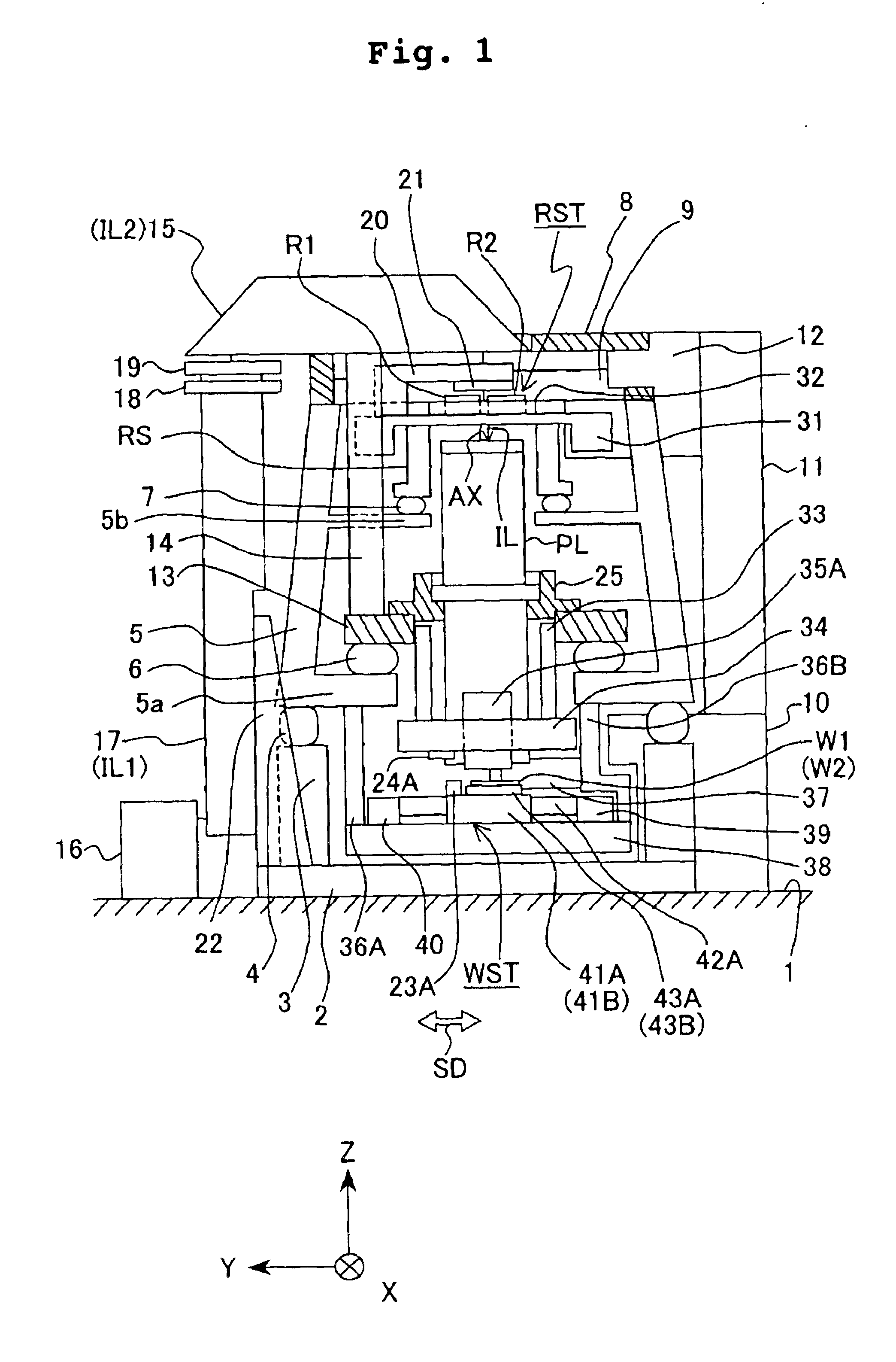
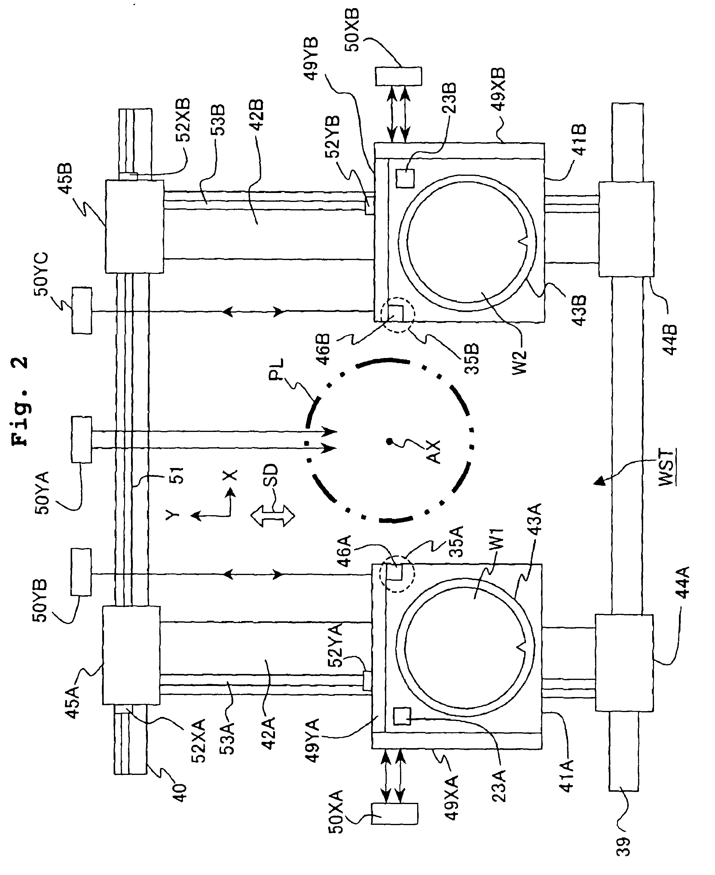
[0018]When the first and second adjustment stages are attached / removed, as mentioned above, it is preferable that the structure of the exposure apparatus is not a structure where each mechanism section is sequentially stacked up on a predetermined base member, but a structure where the stage for the second object is supported by being suspended at the base of the main
body frame, and the stage for the first object is supported at the top section of the main
body frame. This structure is also a structure which can decrease the influence of vibration, so exposure apparatuses having a structure which can decrease the influence of vibration can be efficiently manufactured by the present invention.
[0022]It is also preferable that a partial illumination system (IL2) at the first object side of the illumination system is installed so as to slide with respect to the first main
body frame (90A), so that the partial illumination system is retracted when the first adjustment stage is attached to / removed from the first main body frame and when the stage system is installed. This makes it easier to attach / remove the adjustment stage and to install the stage system.
[0024]In this exposure apparatus, the adjustment stage can be easily mounted instead of the stage system in a state where the partial illumination system is retracted, so the exposure apparatus can be manufactured by the manufacturing method of the exposure apparatuses of the
present method. It is preferable that the stage system further comprise a first stage (RST) and a second stage (WST) which align the first object and the second object respectively, where the second stage is supported by being suspended from the main body frame, and the first stage is supported on the main body frame via the vibration proof member (5 or 7).
[0029]In the above mentioned exposure apparatus, the second stage is supported by being suspended and the first stage is supported to be almost symmetrical to the second stage in the vertical direction, so the influence of vibration is not mutually transferred very much, and the influence of vibration can be decreased. These stages can be easily removed / attached and the adjustment stage can be easily mounted instead of these stages, therefore the exposure apparatus can be manufactured by the manufacturing method for the exposure apparatus of the present invention. In this case, too, if the first stage or the second stage is a double holder type or a
double stage type, the effect of eliminating a large scale dedicated adjustment jig is extremely high.
[0030]In this case, the first stage, for example, is supported by the first member via a third vibration proof member (7). Because of this, the
mutual influence of vibration between the first stage and the second stage is further decreased. Also the first stage, for example, is supported by the second member parallel to the
projection system. In this configuration, too, a vibration proof member exists between the second member and the first member, so the
mutual influence of vibration between the first stage and the second stage is further decreased. It is preferable that a sensor (24A) for detecting the position of at least one of the second stage and second object is installed to the second member, and using the detection information by this sensor, the position of the second stage can be adjusted. The device manufacturing method of the present invention includes a step of transferring a device pattern onto a work piece (W1) using one of the exposure apparatuses of the present invention. By the device manufacturing method of the present invention, high functioning devices can be manufactured at high precision at low cost.

