Method of Forming strained SI/SIGE on insulator with silicon germanium buffer

Inactive Publication Date: 2005-05-17
GLOBALFOUNDRIES INC
View PDF8 Cites 68 Cited by
  • Summary
  • Abstract
  • Description
  • Claims
  • Application Information

AI Technical Summary

Problems solved by technology

The underlying conducting substrate for MOSFETs and bipolar transistors or the interaction of the underlying substrate with the active device regions in CMOS are undesirable features which limit the full performance of high speed devices.
While thermal mixing is a promising method to make strained Si/SiGe-on-insulator, it has draw backs.
Strained Si deposition on SiGe may leave a non-ideal interface with O and C residue, which may affect device performance or yield.
In addition, SiGe

Method used


Image

  • Method of Forming strained SI/SIGE on insulator with silicon germanium buffer
  • Method of Forming strained SI/SIGE on insulator with silicon germanium buffer
  • Method of Forming strained SI/SIGE on insulator with silicon germanium buffer

Examples


Embodiment Construction

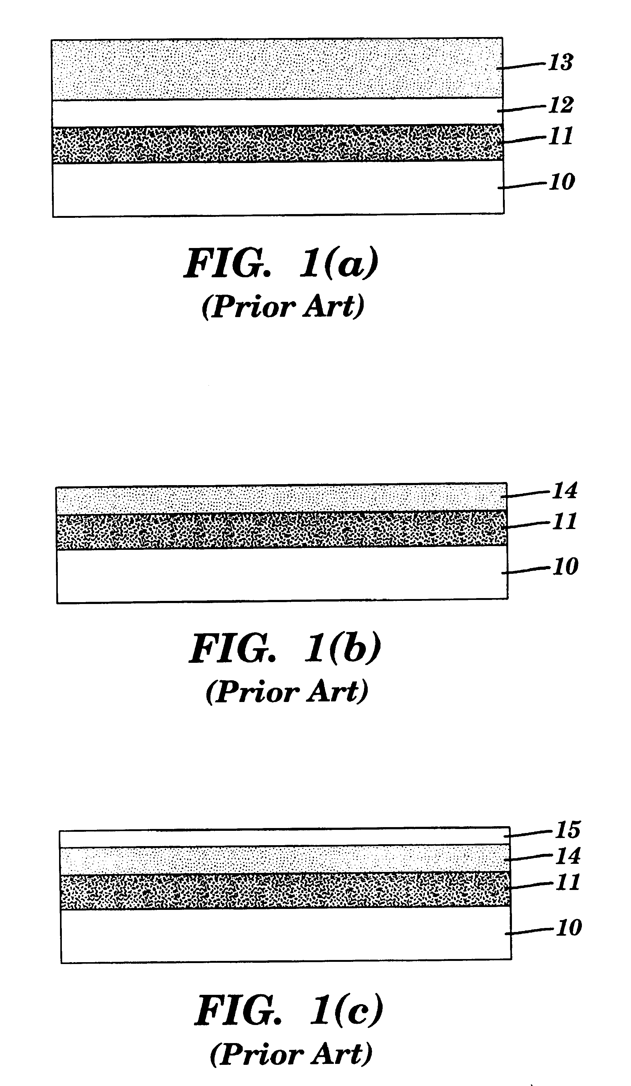
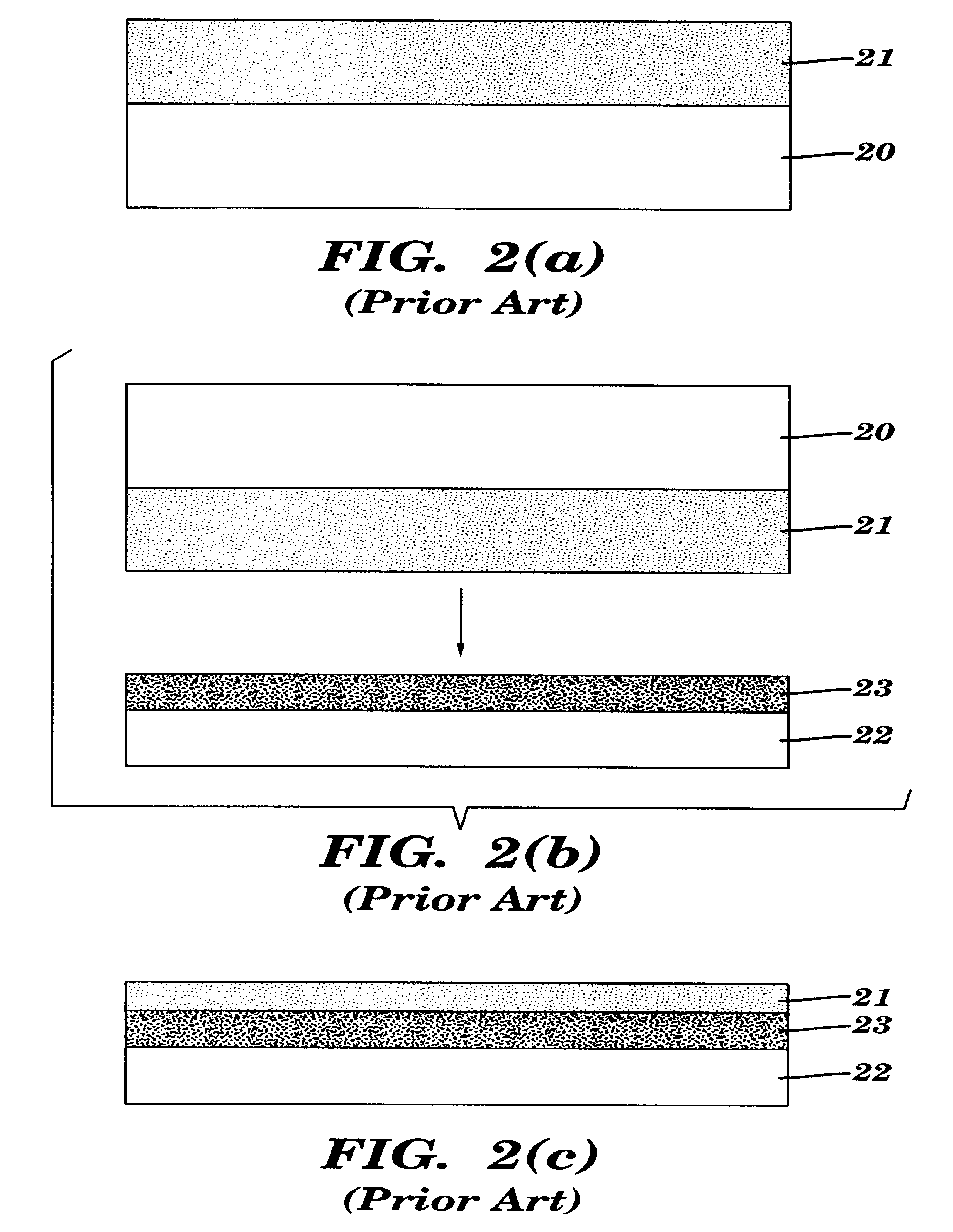
[0018]The invention will now be described by reference to the accompanying figures. In the figures, various aspects of the structures have been shown and schematically represented in a simplified manner to more clearly describe and illustrate the invention. For example, the figures are not intended to be drawn to scale. In addition, the vertical cross-sections of the various aspects of the structures are illustrated as being rectangular in shape. Those skilled in the art will appreciate, however, that with practical structures these aspects will most likely incorporate more tapered features. Moreover, the invention is not limited to constructions of any particular shape.

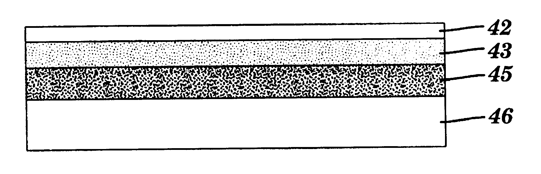
[0019]A preferred embodiment of the method of the present invention is illustrated in FIGS. 4(a)-4(f). The method begins with formation of a relaxed SixGex layer 41 on a first crystalline semiconductor substrate 40, as shown in FIG. 4(a). First substrate 40 may be any single crystal material suitable for forming epit...


PUM


Abstract

A method is disclosed for forming a semiconductor wafer having a strained Si or SiGe layer on an insulator layer. The method produces a structure having a SiGe buffer layer between the insulator layer and the strained Si or SiGe layer, but eliminates the need for Si epitaxy after bonding. The method also eliminates interfacial contamination between strained Si and SiGe buffer layer, and allows the formation of Si/SiGe layers having a total thickness exceeding the critical thickness of the strained Si layer.

Description

BACKGROUND OF INVENTION[0001]This invention relates to integrated circuit (IC) structures and processes that include a strained silicon or silicon germanium (Si / SiGe) layer. More particularly, this invention relates to formation of a structure having a strained Si / SiGe layer on an insulator layer which is useful for fabricating high speed devices such as complementary metal-oxide-semiconductor (CMOS) transistors and other metal-oxide-semiconductor field effect transistor (MOSFET) applications.[0002]Electron and hole mobility in strained silicon or silicon germanium layers has been shown to be significantly higher than that in bulk silicon. For example, measured values of electron mobility in strained Si at room temperature are about 3000 cm2 / Vs as opposed to 400 cm2 / Vs in bulk silicon. Similarly, hole mobility in strained SiGe with high Ge concentration (60%˜80%) reaches up to 800 cm2 / Vs, which is about 5 times the hole mobility in bulk silicon of 150 cm2 / Vs. MOSFETs with strained-S...

Claims


Application Information

Patent Timeline
IPC IPC(8): H01L21/762H01L21/70
CPCH01L21/76254Y10S438/91H01L21/20H01L27/12
Inventor CHEN, HUAJIEBEDELL, STEPHEN W.
Owner GLOBALFOUNDRIES INC
Why Eureka
Try Eureka