Single-electron transistor and fabrication method thereof

a single-electron transistor and fabrication method technology, applied in transistors, nano-level quantum devices, nano-informatics, etc., can solve the problem of inability to control the amount of grown grains, the lithography process has limitations, and the nano-level quantum device cannot meet the width of nano-wires. the effect of reducing the space between the separated gates, reducing the capacitance of the quantum well, and increasing the operating temperature to room temperatur

Inactive Publication Date: 2005-05-17
NAT APPLIED RES LAB
View PDF1 Cites 24 Cited by
  • Summary
  • Abstract
  • Description
  • Claims
  • Application Information

AI Technical Summary

Benefits of technology

[0007]According to this invention, a new method of fabricating the single-electron transistor with self-aligned polysilicon sidewall spacer gates can further reduce space between t...

Problems solved by technology

The self-assembly technology using a natural rule of grain growth can form nano-size grains, but cannot control grain growth on a specific location and the amount of the grown grains.
The lithography process has limitations in the apparatus light source, such that a poor...

Method used


Image

  • Single-electron transistor and fabrication method thereof
  • Single-electron transistor and fabrication method thereof
  • Single-electron transistor and fabrication method thereof

Examples


Embodiment Construction

[0019]The invention will be illustrated in detail by the following preferred embodiments with reference to the accompanying drawings.

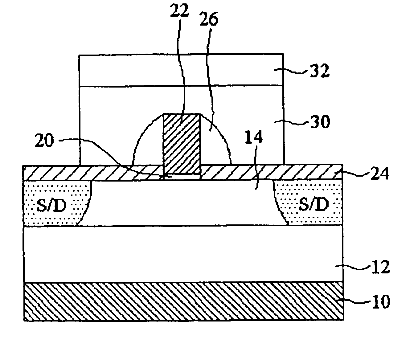
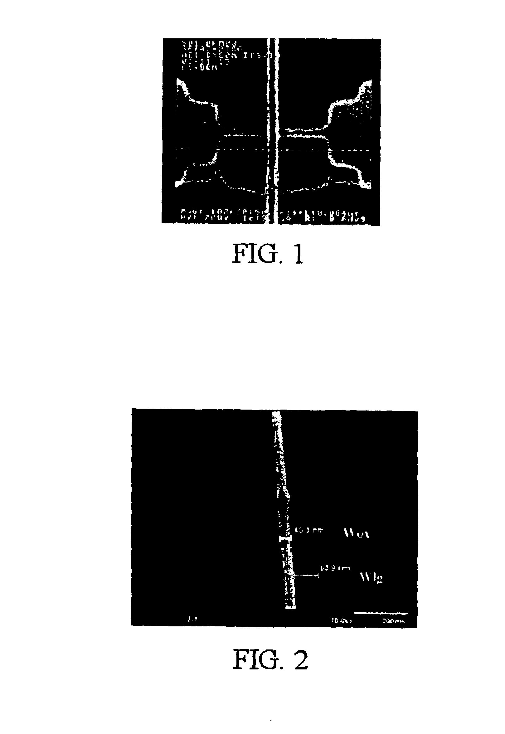
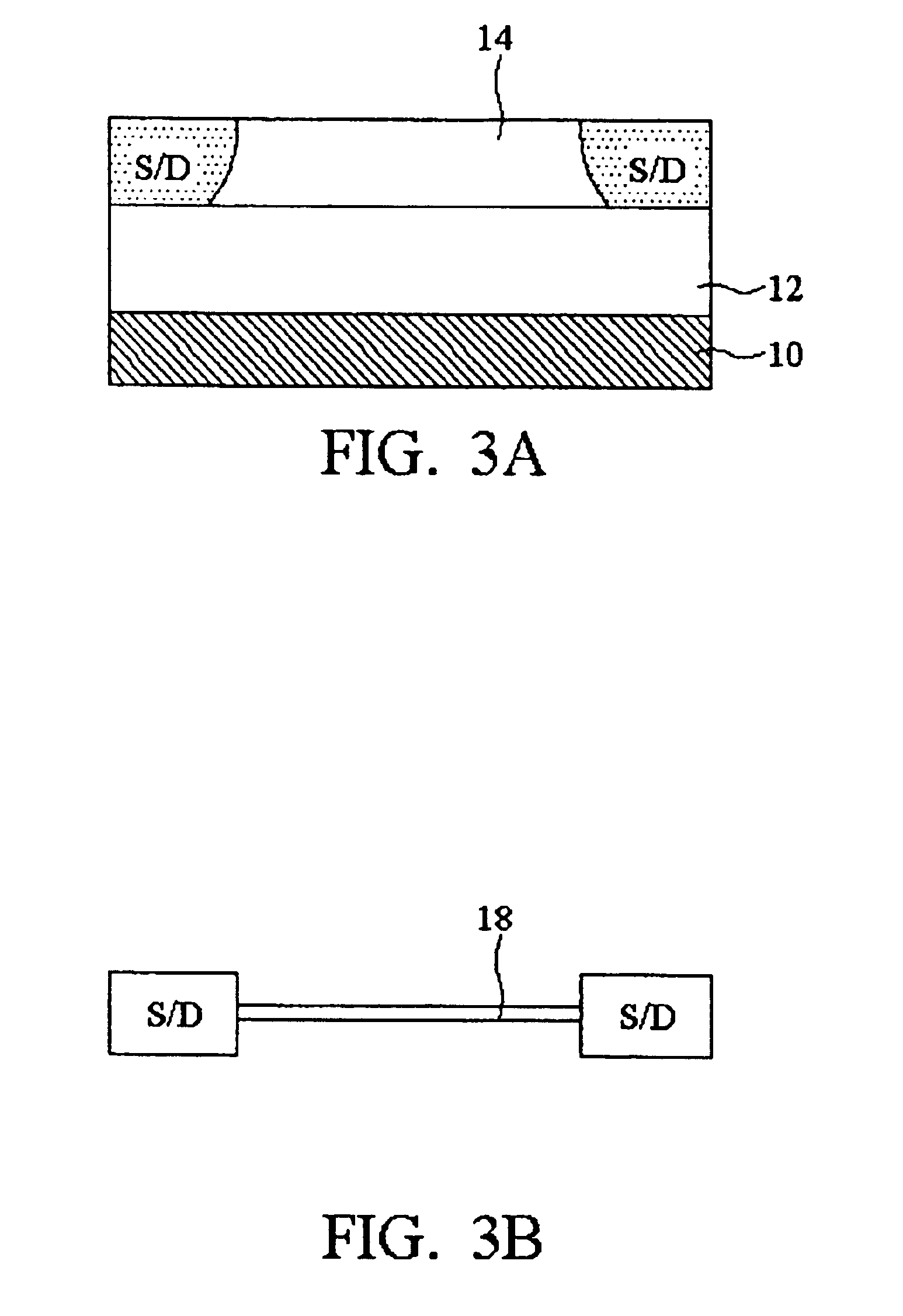
[0020]A nanoscale one-dimensional channel between source and drain on a silicon-on-insulator substrate can be created using electron-beam (E-beam) lithography with multilayer aligned direct writing technology, oxidation and wet etching processes. A one-dimensional silicon dioxide thin wire perpendicularly intersecting the channel is then formed by electron beam (E-beam) lithography and dipping in dilute HF solution to further reduce the width of one-dimensional silicon dioxide thin wire, as shown in FIG. 1. Two potential barriers and a quantum dot capable of charge-storage are created by biasing separated polysilicon sidewall spacer gates to complete a dual-gate controlled single-electron transistor.

[0021]A fabrication method for a single electron transistor in accordance with an embodiment of the present invention is similar to a conventional method f...


PUM


Abstract

A method for fabricating a single-electron transistor (SET). A one dimensional channel is formed between source and drain on a silicon-on-insulator substrate, and the separated polysilicon sidewall spacer gates are formed by electron-beam lithographically etching process in a self-aligned manner. Operation of the single-electron transistor with self-aligned polysilicon sidewall spacer gates is achieved by applying external bias to the self-aligned polysilicon sidewall spacer gates to form two potential barriers and a quantum dot capable of storage charges between the two potential barriers. A metal upper gate is finally formed and biased to induce a two-dimensional electron gas (2DEG) and control the energy level of the quantum well. Accordingly, the method of the invention comprises a combination of electron beam (E-beam) lithography with multilayer-aligned direct writing technology, oxidation, and wet etching to form a nanoscale one-dimensional channel between source and drain on a silicon-on-insulator substrate.

Description

BACKGROUND OF THE INVENTION[0001]1. Field of the Invention[0002]The invention relates to a fabrication method for a single-electron transistor (SET), and more particularly to a single-electron transistor with self-aligned sidewall spacer gates.[0003]2. Description of the Related Art[0004]As semiconductor technology continuously progresses toward a deep sub-micron regime, namely a nanometer scale regime, there has been a tremendous tendency to increase the integration densities of IC devices and decreasing the scale thereof. In general, the fabrication methods for a nanoscale device include an epitaxial growth technique, a self-assembly technology and a lithography process. The epitaxial growth technique is most suitable for III-V group compound semiconductor applications. The self-assembly technology using a natural rule of grain growth can form nano-size grains, but cannot control grain growth on a specific location and the amount of the grown grains. The lithography process has li...

Claims


Application Information

Patent Timeline
IPC IPC(8): H01L29/76H01L21/02H01L29/66H01L21/335
CPCB82Y10/00H01L29/66439H01L29/7613Y10S977/937Y10S438/947
Inventor HU, SHU-FENWU, YUNG-CHUNLU, WEN-TAILIU, SHIUE-SHINHUANG, TIAO-YUANCHAO, TIEN-SHENG
Owner NAT APPLIED RES LAB
Why Eureka
Try Eureka