Diode laser arrangement with a plurality of diode laser arrays

a diode laser and array technology, applied in lasers, laser optical devices, laser construction details, etc., can solve the problems of high demands on liquid-conducting materials, high demands on microchannel heatsinks, and seals

Inactive Publication Date: 2005-05-24
JENOPTIK LASERDIODE
View PDF29 Cites 74 Cited by
  • Summary
  • Abstract
  • Description
  • Claims
  • Application Information

AI Technical Summary

Benefits of technology

[0018]Therefore, it is the primary object of the invention to design a radiation source which can be scaled with respect to power such that different types of cooling can be applied and the configuration of the radiation field is suitable for adapting to different tasks in a simple manner.
[0022]In a particularly advantageous construction, the cooling surface has a step structure and the carriers rest on the steps of the step structure. In an arrangement of this kind, laser radiation is emitted by emission regions which lie next to one another in the array direction of the diode laser arrays and which are arranged so as to be offset by the height of the steps. By means of special optics, it is possible to modify this laser radiation in such a way that a beam quality comparable to that of the stack is achieved. The optics are arranged after the diode laser arrays as a deflecting element which arranges the laser beam bundles adjacent to one another along their elongated extension. The deflecting element comprises a stack of individual elements, each of which is associated with a diode laser line. While one of the side surfaces of the individual element which extend parallel to one another in pairs serves as a beam entry surface, a first end face is constructed as a reflection element which deflects the laser beam bundle in direction of a second end face provided for the beam exit. The extension of the beam entry surface in direction perpendicular to the p-n junction plane exceeds the extension of the collimated laser beam bundle in this direction in such a way that low-attenuation in-coupling of radiation is ensured and reflections are prevented at the side surfaces of the individual element in direction of the fast axis. This ensures that no substantial beam expansion occurs in the individual elements of different length. Due to a divergence of the laser beam bundles in direction of the slow axis, total internal reflection takes place at the respective side surfaces of the individual element, which results in advantageous beam homogenization.
[0023]It is advantageous when the beam entry surface and the end face for the beam exit have an antireflection coating.
[0024]The configuration according to the invention allows the common cooling element to be coupled to a wide variety of heat-dissipating devices such as Peltier elements, a water cooling arrangement or forced convection arrangement. In every case, there should be a heat transmission coefficient of at least 0.03 W / mm2K between the carrier and the cooling surface. Also, the problem of condensation which occurs in the prior art is solved in a simple manner because liquid-guiding channels and seals can be placed outside of a housing provided for the diode laser arrays. Additionally, of course, drying means can be contained or safety arrangements can be integrated in the housing that is provided with an exit area for the laser beam bundles.
[0025]Finally, it can also be advantageous when a collimator for the slow axis parallel to the p-n junction plane is associated with every diode laser line.

Problems solved by technology

Although the direct (active) liquid cooling is extremely effective, the microchannel heatsinks also have drawbacks.
For instance, the structures of the microchannels are complicated to produce.
The coolant, frequently water, places very high demands on the liquid-conducting materials, seals and coolant quality due to the close proximity to the sensitive semiconductor components.
Problems also arise because the liquid-guiding channels must traverse areas with different electric potentials.
If elaborate steps are not taken, very high electrical fields sometimes occur which can trigger highly complex electrochemical processes.
There are also disadvantages connected with the stacking itself.
Finally, the diode stacks have the added disadvantage that they are limited only to determined applications because of the predetermined configuration of their radiation field.

Method used


Image

  • Diode laser arrangement with a plurality of diode laser arrays
  • Diode laser arrangement with a plurality of diode laser arrays
  • Diode laser arrangement with a plurality of diode laser arrays

Examples


Embodiment Construction

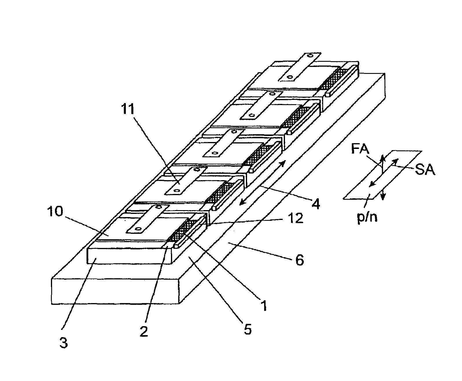
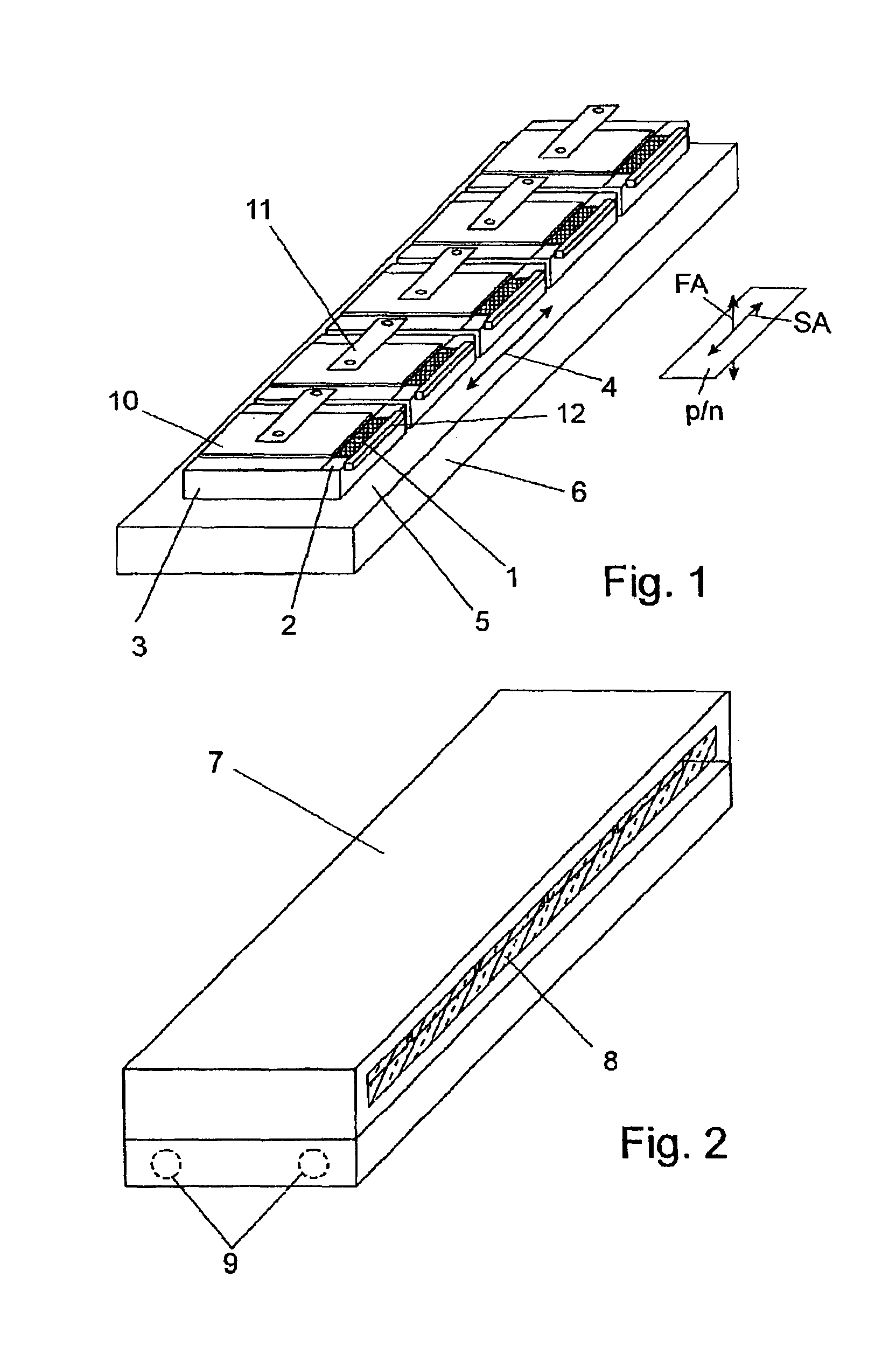
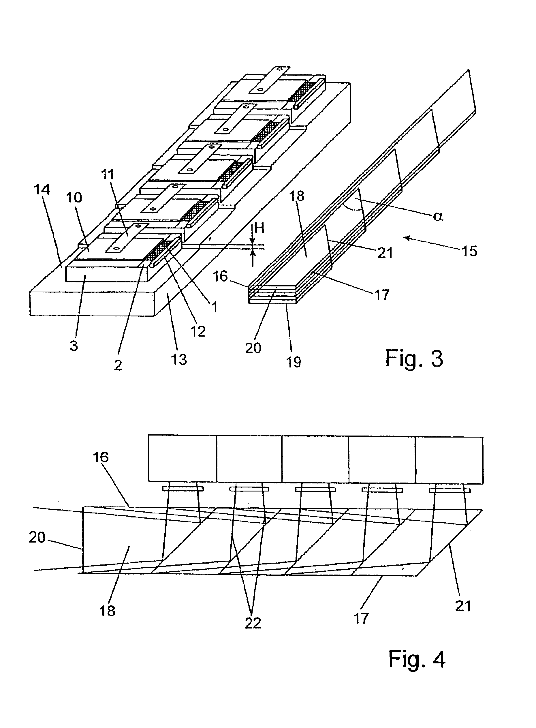
[0039]In the arrangement shown in FIG. 1, diode lasers 1 are provided in the form of diode laser arrays or diode laser bars, each of which is connected to a thermal contact surface 2 of a separate, heat-spreading carrier 3 of copper for dissipating heat. For the sake of clarity, the Figures always show only one of the elements of identical construction. The diode lasers 1 have emission regions which are elongated in one direction, designated by an arrow 4, parallel to the thermal contact surfaces 2. For this reason, the carriers 3 are arranged adjacent to one another and fastened to a cooling surface 5 of a common cooling element 6 so as to be electrically insulated, but with low heat transmission resistance, such that the cooling surface 5 extends parallel to the thermal contact surfaces 2 and the diode lasers 1 lie in a row in their direction of extension and accordingly form a radiation source with a line-shaped laser beam bundle profile. Further, the diode lasers 1 are arranged ...


PUM


Abstract

A diode laser arrangement is disclosed wherein a radiation source is designed which can be scaled with respect to power such that different types of cooling can be applied and the configuration of the radiation field is suitable for adapting to different tasks in a simple manner. For this purpose, every diode laser is connected to a thermal contact surface of a separate, heat-spreading carrier which is fastened to a cooling surface of a common cooling element so as to be electrically insulated. The carriers are arranged adjacently in such a way that the line-shaped emission regions of the diode lasers are adjacent in series and the p-n junction planes extend parallel to the thermal contact surfaces. The diode laser arrangement is particularly suitable as a pump light source.

Description

CROSS-REFERENCE TO RELATED APPLICATIONS[0001]This application claims priority of International Application No. PCT / DE01 / 04398, filed Nov. 21, 2001 and German Application No. 100 61 265.2, filed Dec. 6, 2000, the complete disclosures of which are hereby incorporated by reference.BACKGROUND OF THE INVENTION[0002]1. Field of the Invention[0003]The invention is directed to a diode laser arrangement with a plurality of diode laser arrays, each of which is connected with a thermal contact surface of a heat-spreading carrier and contains a p-n junction plane parallel to the thermal contact surface. The carriers are fastened adjacent to one another in the array direction to a cooling surface of a common cooling element so as to be electrically insulated, so that the cooling surface extends parallel to the thermal contact surfaces.[0004]2. Description of the Related Art[0005]High-power laser diodes which are generally constructed as arrays and are stacked to form two-dimensionally emitting s...

Claims


Application Information

Patent Timeline
IPC IPC(8): H01S5/40H01S5/00H01S5/024
CPCH01S5/4025H01S5/005H01S5/02415H01S5/4018H01S5/4012H01S5/02423
Inventor HENNIG, PETRAHOLLEMANN, GUENTER
Owner JENOPTIK LASERDIODE
Why Eureka
Try Eureka