Polishing systems for use with semiconductor substrates including differential pressure application apparatus

a technology of differential pressure and polishing system, which is applied in the direction of grinding machine components, manufacturing tools, lapping machines, etc., can solve the problems of surface raised “rings”, carrier heads that cannot be adequately compensated, carrier heads that cannot facilitate the application of different amounts of pressure, etc., and achieve constant material removal rate, increase the rate of material removal, and increase the friction at these raised areas

Inactive Publication Date: 2005-05-31
ROUND ROCK RES LLC
View PDF27 Cites 49 Cited by
  • Summary
  • Abstract
  • Description
  • Claims
  • Application Information

AI Technical Summary

Benefits of technology

[0012]In one aspect of the present invention, a surface of a polished semiconductor device structure is analyzed to identify one or more locations thereon where material was removed at a slower rate than remaining locations on the surface. Areas on the surface of the semiconductor device structure where material is removed at decreased rates will typically be higher than, or raised above, other areas on the surface. By increasing the amount of friction between the surface of the semiconductor device structure and a polishing pad at these raised areas, the rate of material removal may be increased. In the present invention, the friction at these raised areas is increased by applying force to the backside of the semiconductor device structure, opposite each raised area on the active surface thereof. The amount of force to be applied to the backside, opposite each raised area, depends upon the height of the raised area relative to the lowest area on the surface of the semiconductor device structure. Thus, the amount of force that is applied to one location or to different locations on the backside of the semiconductor device structure may be determined based on the difference in height between each raised area and the lowest area or areas on the active surface of the semiconductor device structure and by determining the amount of friction needed at each of these areas to provide a substantially constant material removal rate across the entire surface of the semiconductor device structure and to form a substantially planar surface on the semiconductor device structure during polishing thereof.

Problems solved by technology

In addition, although the inhibitors of a slurry function to even out the polishing rate across nonplanar surfaces, polishing of structures with initially great differences in height may not result in a planar surface, but may result in a surface with raised “rings”.
Nonetheless, the carrier heads of Chen do not facilitate the application of different amounts of pressure to different, selected locations on the backside of a semiconductor device structure in response to preventing nonplanarities at specific locations on the active surface of the semiconductor device structure.
Moreover, as the carrier heads of Chen are configured to apply only one or two different amounts of pressure to a semiconductor device structure during polishing thereof, these carrier heads will not adequately compensate for nonplanarities that may be formed during polishing but, rather, may accentuate these nonplanarities.
Accordingly, it appears that the art lacks apparatus for applying selected amounts of pressure to one or more different, selected locations on the backsides of semiconductor device structures during polishing thereof, as well as methods for selectively applying pressure to selected locations on the backside of a semiconductor device structure during polishing thereof.

Method used


Image

  • Polishing systems for use with semiconductor substrates including differential pressure application apparatus
  • Polishing systems for use with semiconductor substrates including differential pressure application apparatus
  • Polishing systems for use with semiconductor substrates including differential pressure application apparatus

Examples


Embodiment Construction

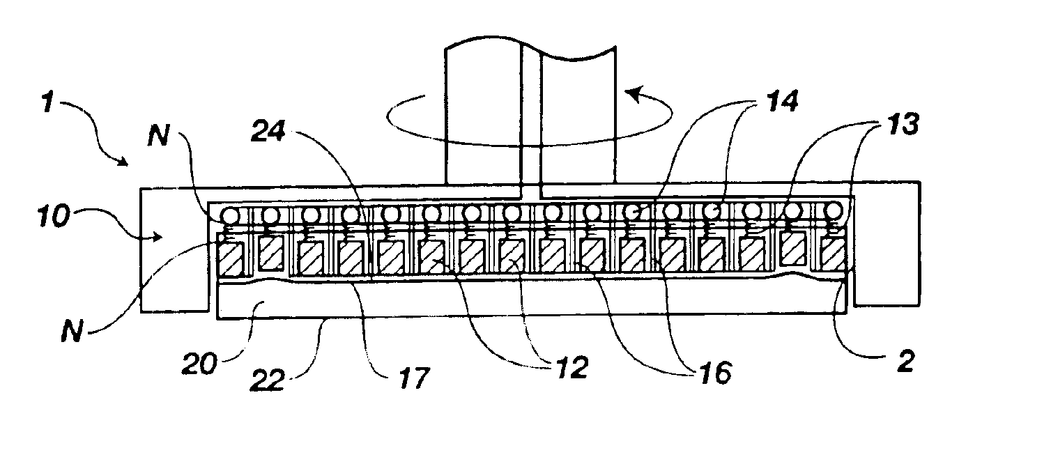
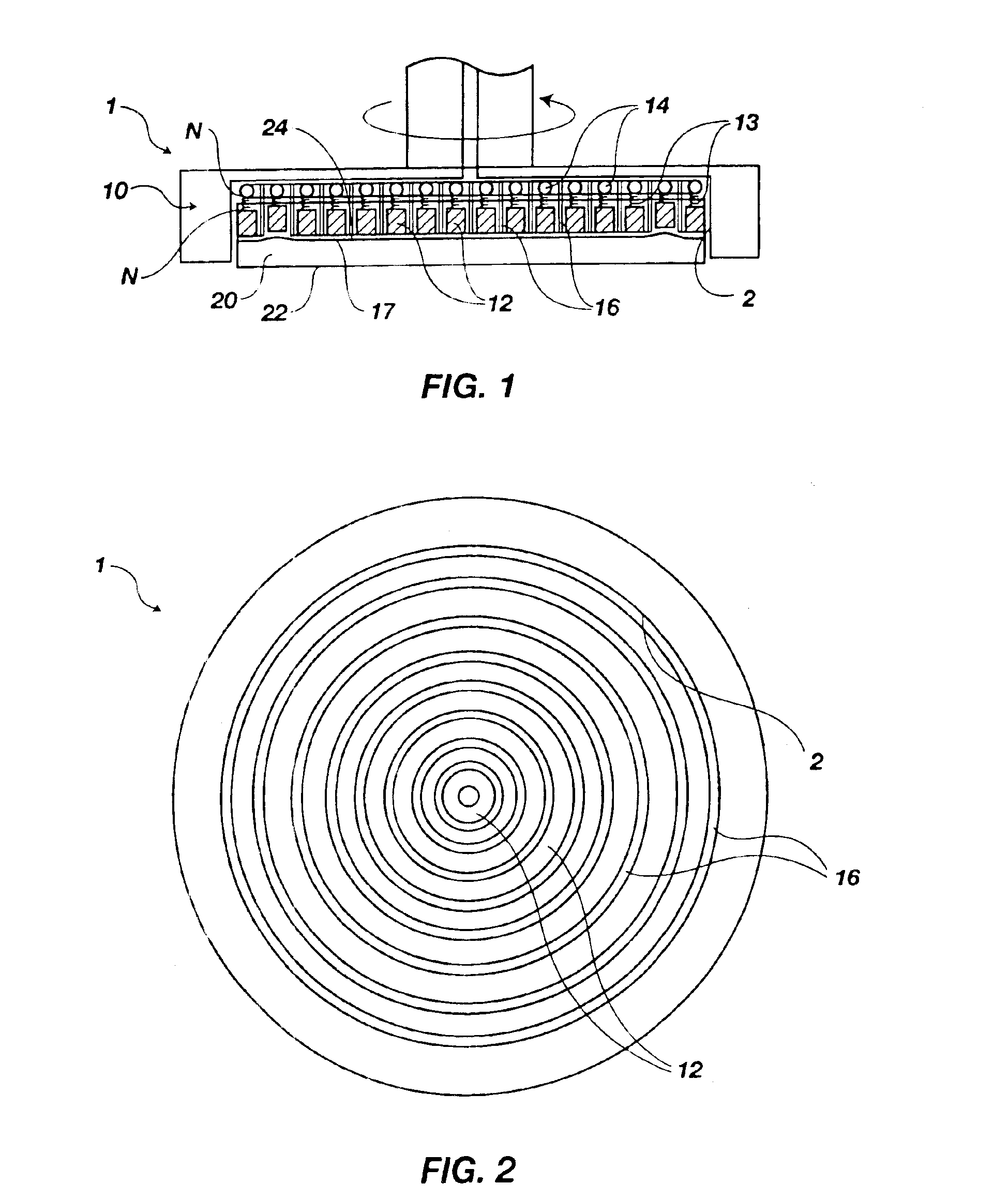
[0034]With reference to FIGS. 1 and 2, a wafer carrier 1 including an exemplary pressure application apparatus 10 that incorporates teachings of the present invention is illustrated. As shown in FIG. 1, pressure application apparatus 10 is located within wafer carrier 1 within a receptacle 2 for receiving at least a backside 24 portion of a semiconductor device structure 20.

[0035]Various types of semiconductor device structures 20 may be assembled with and secured to wafer carrier 1, including, without limitation, full or partial wafers of silicon or other semiconductive materials (e.g., gallium arsenide or indium phosphide), as well as other large-scale substrates (e.g., a silicon-on-insulator (SOI) substrate, such as silicon-on-glass (SOG), silicon-on-ceramic (SOC), silicon-on-sapphire (SOS), or the like).

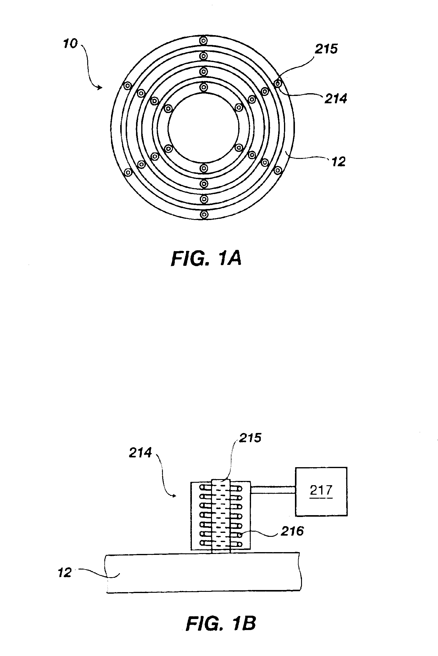
[0036]Pressure application apparatus 10 includes a plurality of independently, substantially vertically movable pressurization structures 12, each of which are configured to be b...


PUM

PropertyMeasurementUnit
forceaaaaaaaaaa
magnetic fieldaaaaaaaaaa
annular shapeaaaaaaaaaa

Abstract

An apparatus for applying different amounts of pressure to different locations of a backside of a semiconductor device structure during polishing thereof. The apparatus is configured to be associated with a wafer carrier of a polishing apparatus and includes pressurization structures configured to be biased against the backside of the semiconductor device structure during polishing thereof. The pressurization structures are independently movable with respect to one another. The amount of force or pressure applied by each pressurization structure to the backside of the semiconductor device structure is controlled by at least one corresponding actuator. The actuator may magnetically facilitate movement of the corresponding pressurization structure toward or away from the backside of the semiconductor device structure. The actuator may alternatively comprise a positive or negative pressure source. Systems including the pressure application apparatus, as well as differential pressure application methods and polishing methods are also disclosed.

Description

CROSS-REFERENCE TO RELATED APPLICATION[0001]This application is a divisional of application Ser. No. 09 / 912,982, filed Jul. 25, 2001, pending.BACKGROUND OF THE INVENTION[0002]1. Field of the Invention[0003]The present invention relates generally to apparatus that apply pressure to the backsides of semiconductor device structures during polishing or planarization of one or more layers thereof. Particularly, the present invention relates to apparatus that selectively apply different amounts of pressure to different locations on the backsides of semiconductor device structures as one or more layers on the opposite, active surfaces thereof are polished or planarized. More particularly, the present invention relates to apparatus that employ magnetic fields to independently apply pressure to different, selected locations on the backside of a semiconductor device structure. The present invention also relates to polishing methods wherein different amounts of pressure are selectively applied...

Claims


Application Information

Patent Timeline
Patent Type & Authority Patents(United States)
IPC IPC(8): B24B37/04B24B41/06H01L21/02H01L21/306B24B7/00B24B37/30B24B49/16
CPCB24B1/005B24B37/30B24B49/16Y10T29/41H01L21/30625
Inventor BROWN, NATHAN R.
Owner ROUND ROCK RES LLC
Why Eureka
Try Eureka