Solid-state imaging device

a solid-state imaging and imaging device technology, applied in the direction of radiological control devices, instruments, television systems, etc., can solve the problems of reducing the thickness of the on-chip microlens inclusive of the convex lens, affecting the light transmittivity, and reducing the film so as to facilitate the process control, reduce the thickness of the on-chip microlens, and enhance the effect of light transmission efficiency

Inactive Publication Date: 2005-05-31
SONY CORP
View PDF4 Cites 36 Cited by
  • Summary
  • Abstract
  • Description
  • Claims
  • Application Information

AI Technical Summary

Benefits of technology

[0019]It is therefore an object of the present invention to provide a solid-state imaging device adapted for reducing the film thickness of an on-chip microlens with regard to the area of each unit pixel and also for enhancing the light transmission efficiency while facilitating the process control.

Problems solved by technology

However, in the above conventional solid-state imaging device where the on-chip microlens 18 is formed into a single convex lens 18A correspondingly to one unit pixel (light receiving part of the photodiode 12) 10, the device functions effectively in case the area of the unit pixel is small, but the following problems arise when the unit pixel has a relatively large area.
First, if a spherical lens is employed in particular for enabling a single convex lens to cover the entire light receiving region of one unit pixel, it is necessary to ensure a large radius of the on-chip microlens, i.e., to increase the height of the microlens, hence requiring a process of machining the microlens by the use of a thick material film to consequently bring about some difficulty in the process control.
Further, the film thickness of the on-chip microlens inclusive of the convex lens is rendered great to eventually exert harmful influence on the light transmittivity.
However, even in such a shape, it is still impossible to eliminate the difficulty in the process control.
First, in the solid-state imaging device of this kind, any of wiring and the like for the peripheral circuit is not permitted in the light receiving part of the photodiode so as to secure an optical path therein. That is, the circuit wiring needs to be laid out in some other region than the light receiving part of the photodiode, hence enlarging the size of each unit pixel and reducing the aperture ratio which represents the rate of the area of the light receiving part to the pixel size.

Method used


Image

  • Solid-state imaging device
  • Solid-state imaging device
  • Solid-state imaging device

Examples


first embodiment

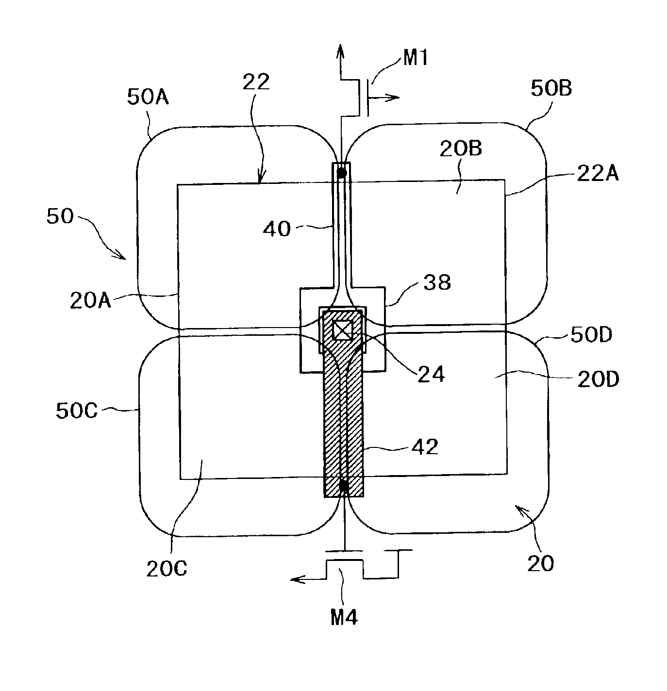
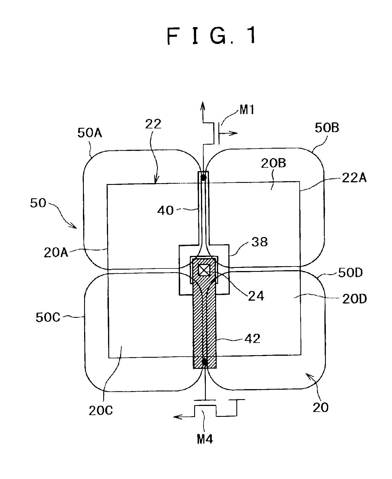
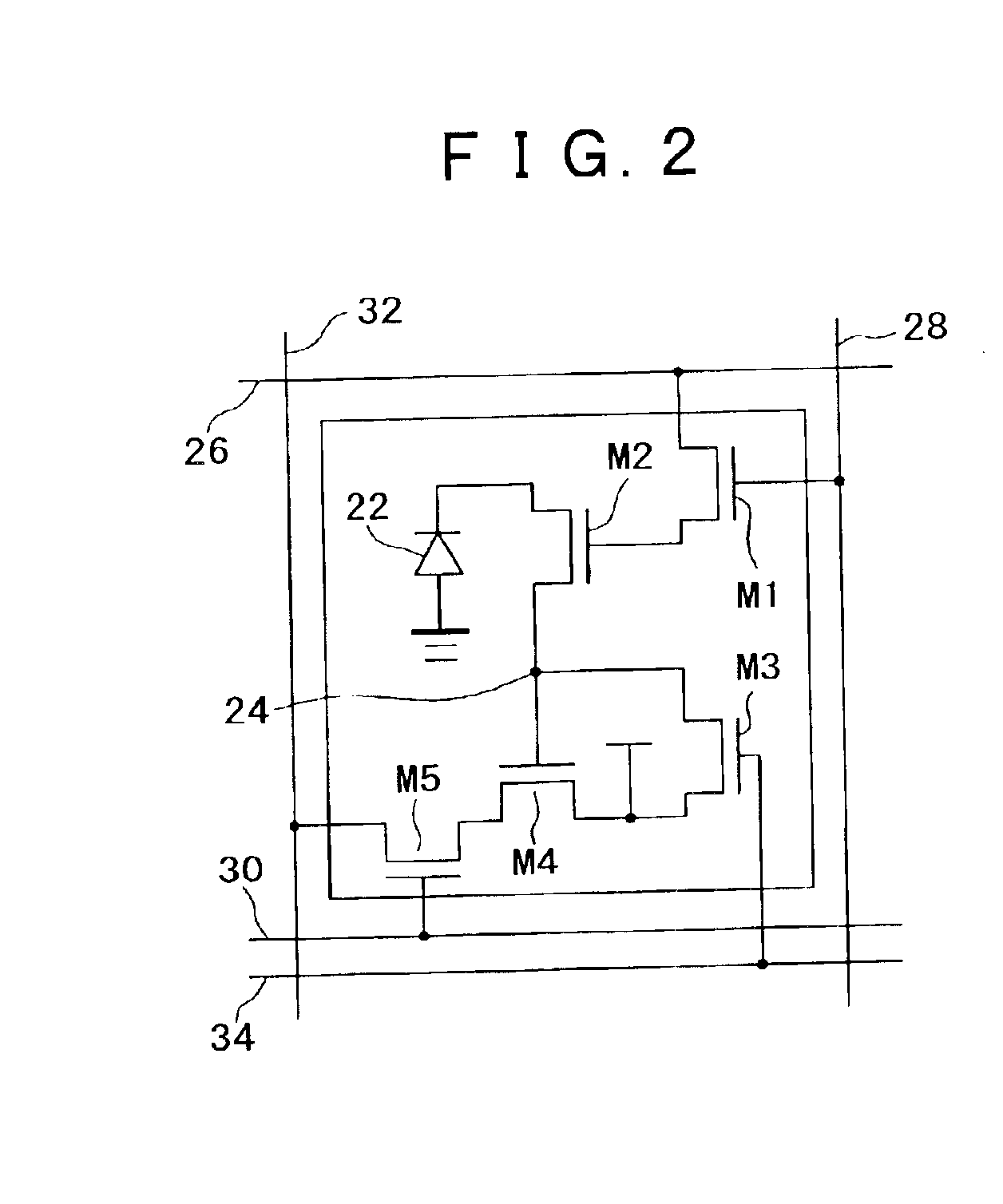
[0033]FIG. 1 is a schematic partial plan view showing an exemplary layout of an on-chip microlens in the solid-state imaging device according to the present invention, and FIG. 2 is a circuit diagram showing a circuit configuration of a unit pixel in the solid-state imaging device of FIG. 1.

[0034]The embodiment shown in these diagrams represents one case of applying the present invention to a CMOS type image sensor. Referring first to FIG. 2, an explanation will be given on the structure of a unit pixel in this embodiment.

[0035]As shown in FIG. 2, the unit pixel 20 includes one photodiode 22 and five MOS transistors M1-M5.

[0036]The photodiode 22 generates a signal charge in proportion to the amount of incident light from a light receiving part and then stores the charge therein. In response to a pulse signal supplied via a transfer line 26 and a column selection line 28, the read transistor M2 and the address transistor M1 transfer the signal charge, which is stored in the photodiod...

second embodiment

[0056]FIG. 3 is a schematic partial plan view showing an exemplary layout of an on-chip microlens in the solid-state imaging device according to the present invention. Any components common to those shown in FIG. 1 are denoted by the same reference numerals or symbols, and a repeated explanation thereof will be omitted below.

[0057]This solid-state imaging device has, in addition to the aforementioned structure of FIG. 1, an upper-layer metal wiring 44 along the respective boundaries of convex lens parts 50A, 50B, 50C and 50D of an on-chip microlens.

[0058]The metal wiring 44 is composed of aluminum or the like and is disposed orthogonally to the aforementioned wirings 40 and 42.

[0059]More specifically, the wirings 40, 42 and 44 are disposed by using the entire cross boundaries which are formed by the convex lens parts 50A, 50B, 50C and 50D.

[0060]Such upper-layer wiring 44 may be utilized for control of the various transistors and also for power supply, grounding or the like.

third embodiment

[0061]FIG. 4 is a schematic partial plan view showing an exemplary layout of an on-chip microlens in the solid-state imaging device according to the present invention. Any components common to those shown in FIG. 1 are denoted by the same reference numerals or symbols, and a repeated explanation thereof will be omitted below.

[0062]This solid-state imaging device has, on a photodiode 22, a cross-shaped light shield wiring 46 formed along the respective boundaries of convex lens parts 50A, 50B, 50C and 50D of the microlens 50 for preventing diffused reflection of the light or any stray light.

[0063]The light shield wiring 46 is normally used for power supply and, since it is shaped into a cross, the power supply wiring area can be enlarged to consequently achieve an effect of diminishing the potential fall caused in the case of a current flow.

[0064]Due to the structure mentioned above, it becomes possible to set the circuit wirings 40, 42, 44 and 46 on the photodiode 22 without the nec...


PUM


Abstract

A solid-state imaging device having, in each of unit pixels, an on-chip microlens composed of plural convex lens parts for each of photoelectric conversion elements provided on a semiconductor chip is disclosed. A floating diffusion part and a signal-charge read gate for taking out a signal charge from the photoelectric conversion element are provided on a region positioned in a boundary of each convex lens part of the on-chip microlens. A wiring for the floating diffusion part and a wiring for the read gate are provided along the respective boundaries of the convex lens parts of the on-chip microlens. In this device, the film thickness of the on-chip microlens can be reduced with regard to the area of each unit pixel, thereby facilitating the process control and enhancing the light transmission efficiency. It is also possible to enhance the circuit wiring efficiency in each unit pixel while avoiding any incomplete charge transfer to consequently improve the picture quality.

Description

[0001]This application claims priority to Japanese Patent Application Number JP2002-012568 filed Jan. 22, 2002, which is incorporated herein by reference.BACKGROUND OF THE INVENTION[0002]The present invention relates to a solid-state imaging device such as a CCD type image sensor or a CMOS type image sensor where an on-chip microlens is mounted on a semiconductor chip having plurality of photoelectric conversion elements.[0003]It has been known heretofore that a solid-state imaging device such as a CCD or CMOS type image sensor has a plurality of photodiodes (photoelectric conversion elements) arranged in a two-dimensional array, wherein a signal charge generated by each photodiode is converted into an electric signal by a peripheral element and then is outputted therefrom.[0004]That is, in a CCD type image sensor, a signal charge obtained from each photodiode is transferred by a CCD vertical transfer register and a CCD horizontal transfer register, and then is converted into an ele...

Claims


Application Information

Patent Timeline
Patent Type & Authority Patents(United States)
IPC IPC(8): G02B3/00H01L27/148H01L27/14H01L27/146H01L31/10H04N5/335H01L31/0232H01L31/062H04N5/369H04N5/374
CPCH01L27/14603H01L27/14627H01L27/14609
Inventor SUGIYAMA, TOSHINOBU
Owner SONY CORP
Why Eureka
Try Eureka