Thin film transistor array panel for a liquid crystal display

Inactive Publication Date: 2005-05-31
SAMSUNG DISPLAY CO LTD
View PDF3 Cites 38 Cited by
  • Summary
  • Abstract
  • Description
  • Claims
  • Application Information

AI Technical Summary

Benefits of technology

[0010]It is an object of the present invention to reduce pixel defects by preventing shorts between pix

Problems solved by technology

However, in the process of manufacturing the panels for the liquid crystal display, if a conductive material remains on an unintended portion of the panel, in particular between adjacent pixel electrodes or between the pixel electrodes and the data lines, a pixel defect occurs in which the pixels remain in a white state even when the same are controlled to an OFF state.
This is a result of shorting of the pixel electrodes with the data lines or adjacent pixel electrodes.
This results in an overall r

Method used


Image

  • Thin film transistor array panel for a liquid crystal display
  • Thin film transistor array panel for a liquid crystal display
  • Thin film transistor array panel for a liquid crystal display

Examples


first embodiment

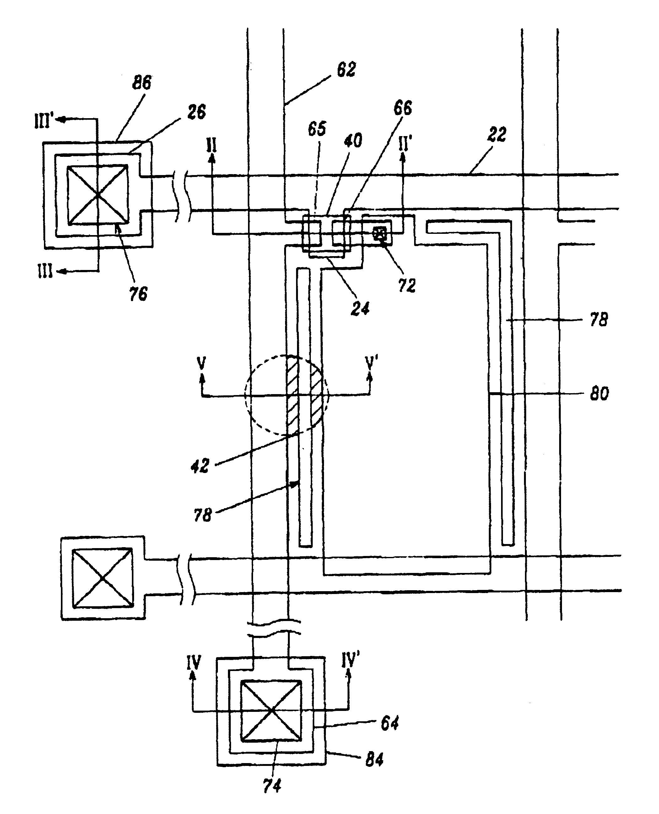
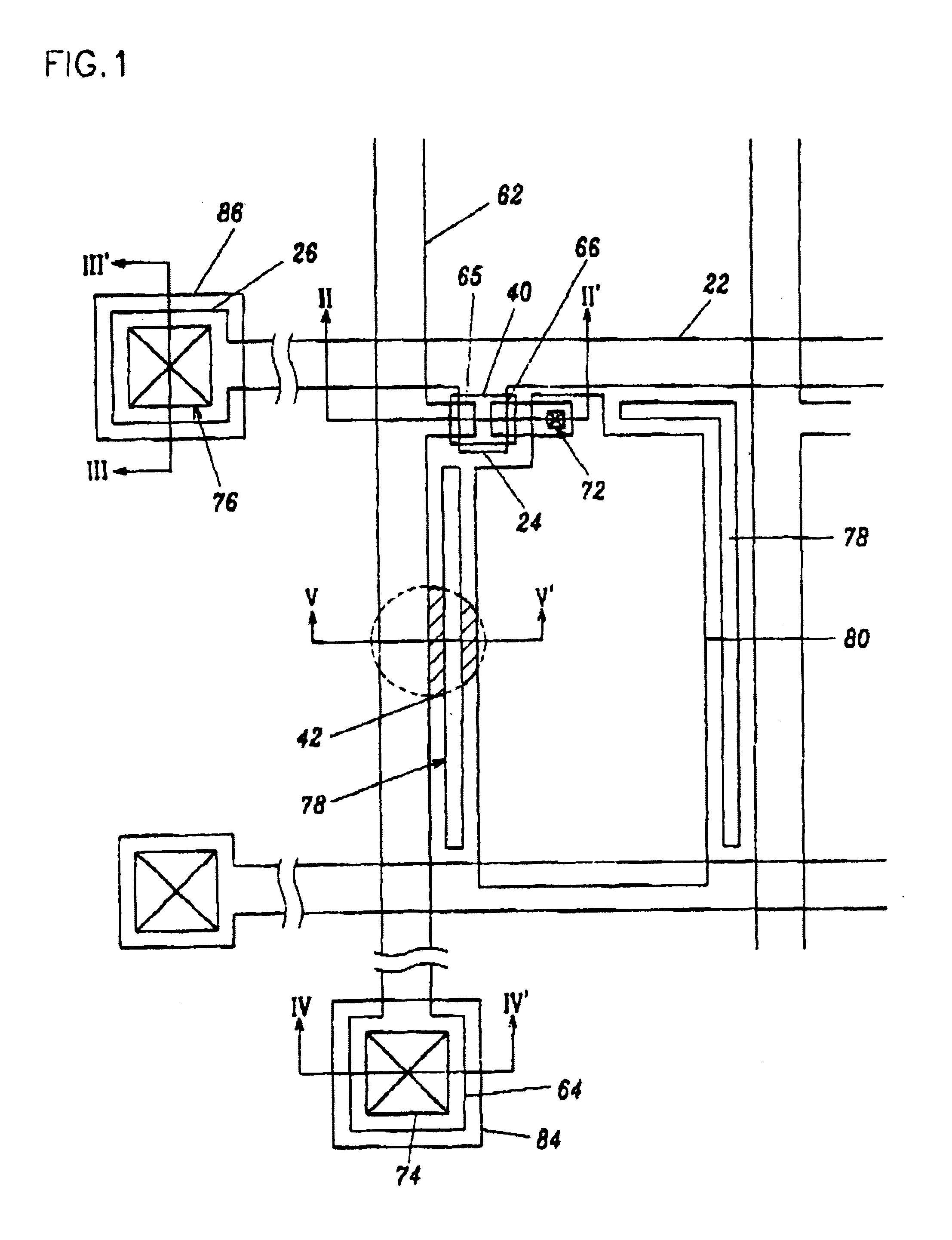
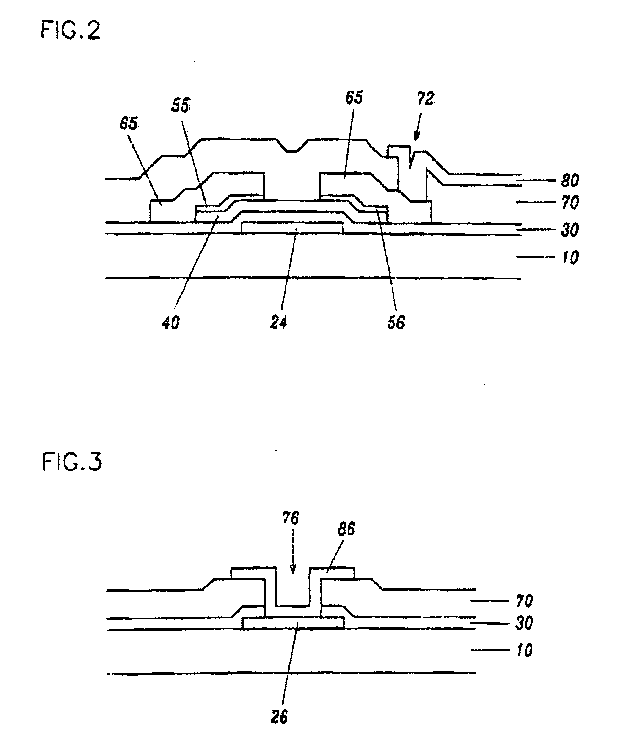
[0059]FIG. 1 is a layout view of a thin film transistor array panel for a liquid crystal display according to the present invention, FIG. 2 is a cross-sectional view of a thin film transistor taken along line II-II′ of FIG. 1, FIG. 3 is a cross-sectional view of a gate pad taken along line III-III′ of FIG. 1, FIG. 4 is a cross-sectional view of a data pad taken along line IV-IV of FIG. 1, and FIG. 5 is a cross-sectional view taken along line V-V′ of FIG. 1.

[0060]As shown in FIGS. 1 to 5, a gate line (or scanning signal line) 22 extending in the horizontal direction is formed on an insulating substrate 10; a gate pad 26 is formed connected to an end of the gate line 22, the gate pad 26 transmitting a scanning signal from an external circuit to the gate line 22; and a gate electrode 24, which is part of a thin film transistor, is formed branched from the gate line 22. Also, a gate insulating layer 30 of silicon-nitride (SiNx) is formed on the gate wire parts 22, 24, and 26 and covers ...

second embodiment

[0079]A structure of a thin film transistor array panel having a dual-gate line according to the present invention will now be described with reference to FIGS. 8 and 9.

[0080]FIG. 8 is a layout view of a thin film transistor array panel for a liquid crystal display having a dual-gate line according to the second embodiment of the present invention, and FIG. 9 is a cross-sectional view of a thin film transistor taken along line IX-IX′ of FIG. 8.As shown in FIGS. 8 and 9, because openings 77 and 78 in the vertical direction are formed between a data line 62 and a pixel electrode 80 or between the data line 62 and a connection portion 27, remaining conductive material 43, which remains between the data line 62 and the pixel electrode 80, or the pixel electrode 80 and an adjacent pixel electrode, is separated into two portions 431 and 432. That is, because the portion 431, which contacts the data line 62, and the portion 432, which contacts or overlaps the pixel electrode 80, are separa...

third embodiment

[0083]FIG. 10 is a layout view of a thin film transistor array panel for a liquid crystal display according to the present invention, FIG. 11 is a cross-sectional view of a thin film transistor taken along line XI-XI′ of FIG. 10, FIG. 12 is a cross-sectional view taken along line XII-XII′ of FIG. 10, FIG. 13 is a cross-sectional view of a gate pad taken along line XIII-XIII′ of FIG. 10, and FIG. 14 is a cross-sectional view of a data pad taken along line XIV-XIV′ of FIG.

[0084]As with the above embodiments, a gate line (or scanning signal line) 22 extending in the horizontal direction, a gate pad 26, and a gate electrode 24 are formed on an insulating substrate 10. A gate insulating layer 30 is formed on is the gate wire parts 22, 24, and 26 to cover the same, and has a contact hole 36 exposing the gate pad 26. A semiconductor layer 40 made of hydrogenated amorphous silicon and an ohmic contact layer 55 and 56 made of hydrogenated amorphous silicon doped with Ntype impurities are for...


PUM


Abstract

A gate wire including a gate line extending in the horizontal direction, and a gate electrode is formed on an insulating substrate. A gate insulating layer is formed on the gate wire and covers the same. A semiconductor pattern is formed on the gate insulating layer 30, and formed on the semiconductor pattern are a data wire having a date line in the vertical direction, a source electrode, a drain electrode separated from the source electrode opposite the source electrode with respect to the gate electrode, and an align pattern located on both sides of the data line. A passivation layer is formed on the data wire and the align pattern, and has contact holes exposing the drain electrode and an opening exposing the substrate between the data line and the align pattern. Here, the align pattern adjacent to the data line is exposed through the opening, and the semiconductor pattern and the gate insulating layer are under-cut. A pixel electrode connected to the drain electrode through the contact hole is formed on the passivation layer. Here, the opening is located between the data line and the pixel electrode. In this structure, misalignment occurring in the manufacturing process of a thin film transistor panel for a liquid crystal display is minimized, and stitch defects are prevented by uniformity forming a coupling capacitance between the data line and the pixel electrode. Shorts between the data line and the pixel electrode are prevented by forming the opening between the data line and the pixel electrode.

Description

[0001]This is a divisional application of the U.S. patent application Ser. No. 09 / 450,333 filed on Nov. 29, 1999, which has become U.S. Pat. No. 6,798,442.BACKGROUND OF THE INVENTION[0002](a) Field of the Invention[0003]The present invention relates to a thin film transistor array panel for a liquid crystal display and a method of manufacturing the same.[0004](b) Description of the Related Art[0005]Liquid crystal display (LCDs) are one of the most widely used flat panel display (FPD) configurations. The liquid crystal display has two panels having electrodes for generating an electric field and a liquid crystal layer interposed between the two panels. The transmittance of incident light is controlled by the intensity of the electric field applied to the liquid crystal layer.[0006]The typical liquid crystal display uses a thin film transistor as a switching element. Data lines and gate lines, which cross each other to define pixels in a matrix array, are formed on the panel on which ...

Claims


Application Information

Patent Timeline
IPC IPC(8): G02F1/13G02F1/1343G02F1/1362H01L21/77H01L21/84H01L29/10H01L29/12
CPCG02F1/134336G02F1/1362G02F1/136286H01L27/1288H01L29/12H01L27/124G02F2001/13606G02F1/13606
Inventor KIM, DONG-GYUSONG, JUN-HOCHANG, JONG-WOONGCHOI, JAE-HONA, BYOUNG-SUNPARK, YOUNG-BAEHUH, SUNG-WOOK
Owner SAMSUNG DISPLAY CO LTD
Why Eureka
Try Eureka