SiGe strain relaxed buffer for high mobility devices and a method of fabricating it

a buffer and high mobility technology, applied in the field of sige strain relaxed buffer for high mobility devices and a method of fabricating it, can solve the problems of low level of integration possible on these wafers, lack of natural oxide such as siosub>2/sub>, and insufficient high frequency and opto-electronic properties of conventional silicon based devices, etc., to achieve a simple and reliable method of growing tsrb

Active Publication Date: 2005-06-14
INTERUNIVERSITAIR MICRO ELECTRONICS CENT (IMEC VZW) +1
View PDF8 Cites 39 Cited by
  • Summary
  • Abstract
  • Description
  • Claims
  • Application Information

AI Technical Summary

Benefits of technology

[0017]The preferred embodiments provide a SiGe strain relaxed buffer (TSRB) with improved features for hi

Problems solved by technology

Since new applications are focused on wireless and optical communication, conventional silicon based devices do not offer any more sufficient high frequency and opto-electronic properties.
Until now high frequency and optical applications mostly have been outclassed by the III-V materials grown on GaAs wafer, but the lack of natural oxide such as SiO2 and the low level of integration possible on these wafers are major drawbacks.
The main challenge is then to deposit these materials on a substrate, which has a different lattice parameter.
The lattice mismatch between the film and the substrate gives rise to the formation and the propagation of dislocations into the epilayer.
Each dislocation in the active part of the epitaxial layer leads to the deteriorat

Method used


Image

  • SiGe strain relaxed buffer for high mobility devices and a method of fabricating it
  • SiGe strain relaxed buffer for high mobility devices and a method of fabricating it
  • SiGe strain relaxed buffer for high mobility devices and a method of fabricating it

Examples


Embodiment Construction

[0057]The following description and examples illustrate a preferred embodiment of the present invention in detail. Those of skill in the art will recognize that there are numerous variations and modifications of this invention that are encompassed by its scope. Accordingly, the description of a preferred embodiment should not be deemed to limit the scope of the present invention.

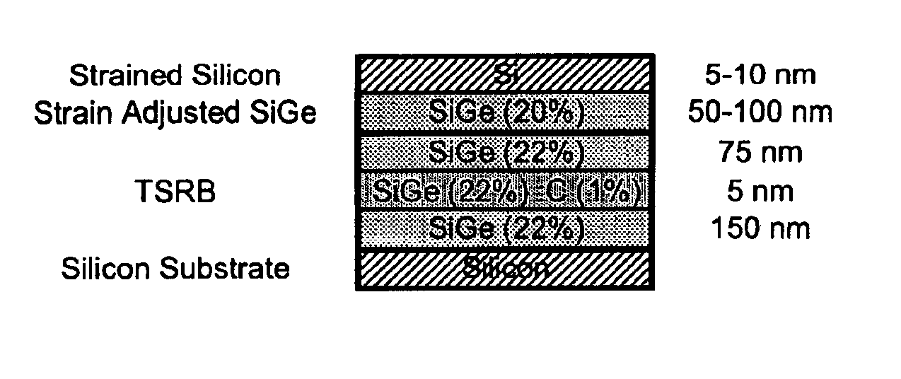
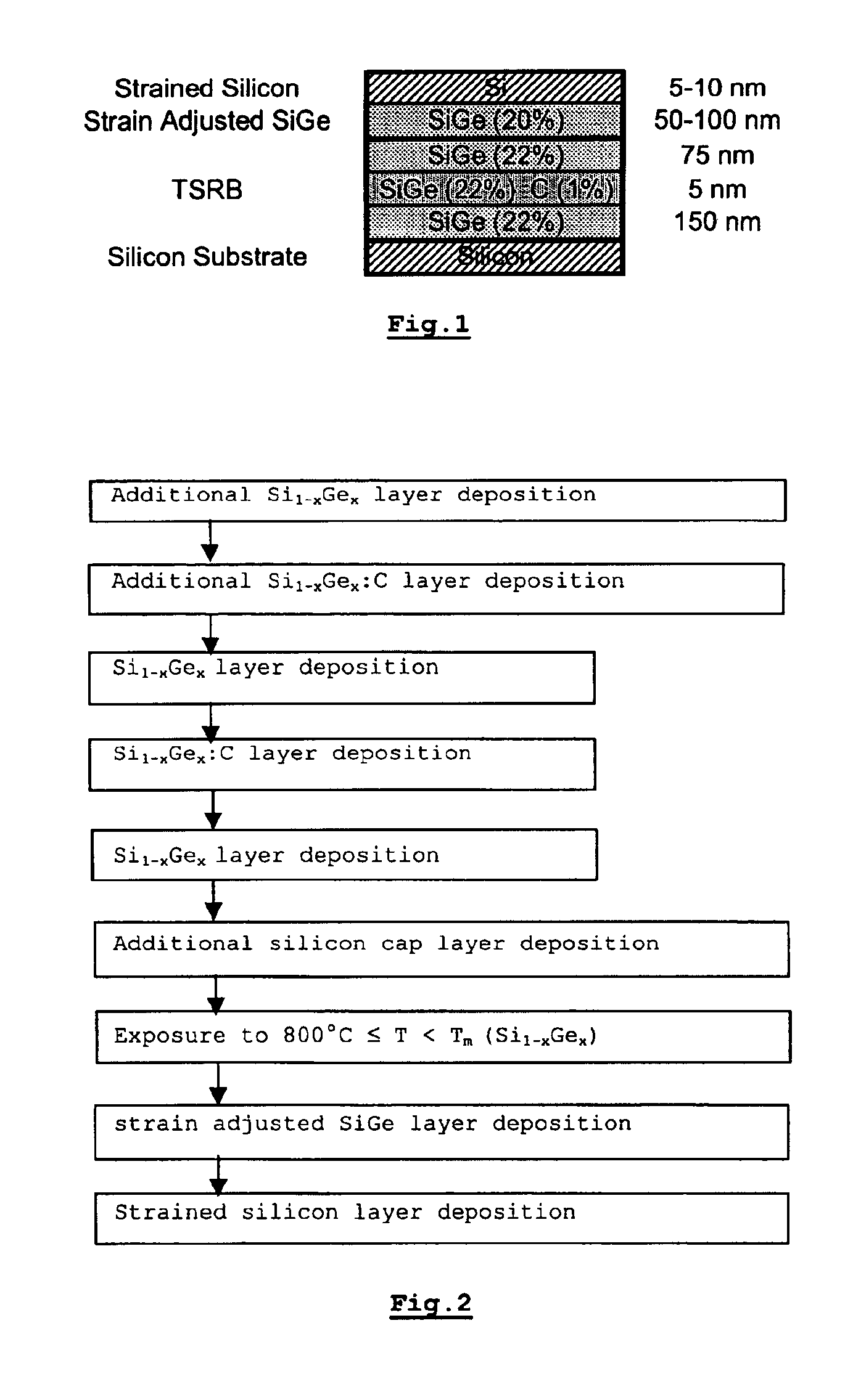
[0058]The preferred embodiments relate to a Thin Strain Relaxed Buffer (TSRB) for the integration of high mobility devices (for example SiGe / strained Si system) on top of a semiconductor substrate like e.g. Silicon. In the following description both the Thin Strain Relaxed Buffer and the method to obtain it are explained.

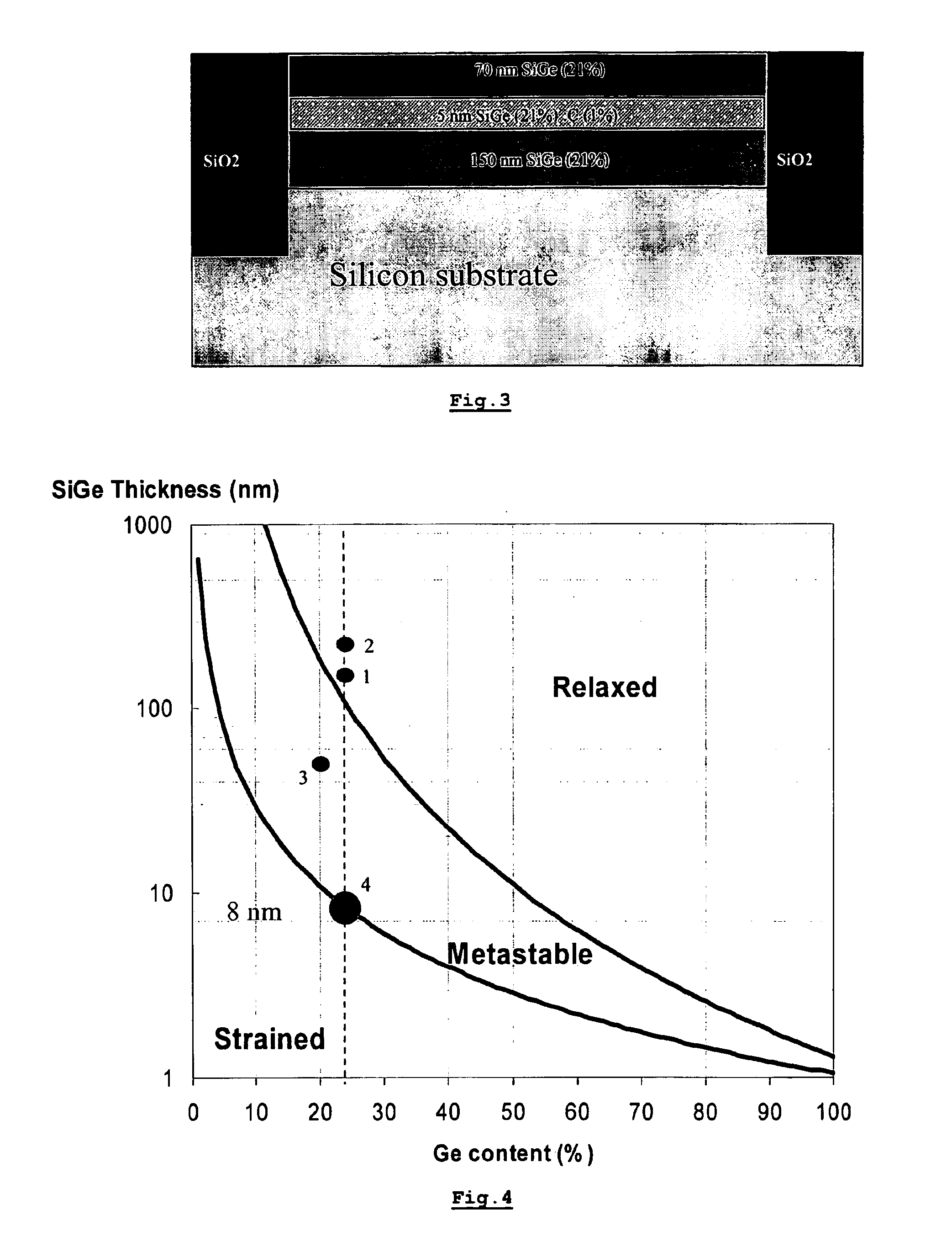
[0059]One grows epitaxially a TSRB based on Si0.78Ge0.22 / Si0.78Ge0.22:Cy / Si0.78Ge0.22 multilayer system, with y (C concentration) at least 0.3% and preferably between 0.5% and 1%. 91% relaxation was reached after rapid thermal annealing (30″ at 1000° C.) of the TSRB, with a very smooth surfa...


PUM


Abstract

A semiconductor device is provided comprising a semiconductor substrate having on its top a Thin Strain Relaxed Buffer. The Thin Strain Relaxed Buffer consists of a stack of three layers of essentially constant Ge concentration. The three layers include a first epitaxial layer of Si1-xGex, a second epitaxial layer of Si1-xGex:C, and a third epitaxial layer of Si1-xGex on the second epitaxial layer. A method to fabricate such a buffer is also provided.

Description

RELATED APPLICATION[0001]This application claims the benefit of U.S. Provisional Application No. 60 / 440,400, filed Jan. 14, 2003, the contents of which is hereby incorporated by reference in its entirety.FIELD OF THE INVENTION[0002]An epitaxial multilayer buffer suitable for the creation of high mobility devices on top of a semiconductor substrate is provided. A method to fabricate such a buffer is also provided.BACKGROUND OF THE INVENTION[0003]For years, digital electronics has been dominated by Si / SiO2 based technology, because of the low cost of silicon and the properties (structural and electronic) of the Si / SiO2 system. Since new applications are focused on wireless and optical communication, conventional silicon based devices do not offer any more sufficient high frequency and opto-electronic properties. Nowadays, two materials / systems have the functionality required for these new applications: III-V materials (InP, GaAs, and the like) and IV-IV heterostructures (SiGe / Si).[000...

Claims


Application Information

Patent Timeline
IPC IPC(8): H01L29/02H01L29/10H01L21/20
CPCH01L21/02381H01L21/02447H01L21/0245H01L29/107H01L21/0262H01L21/02636H01L29/1054H01L21/02532H01L21/02505H01L21/02667
Inventor DELHOUGNE, ROMAINLOO, ROGERMEUNIER-BEILLARD, PHILIPPECAYMAX, MATHIEU
Owner INTERUNIVERSITAIR MICRO ELECTRONICS CENT (IMEC VZW)
Why Eureka
Try Eureka