Active matrix display device and manufacturing method thereof

a technology of active matrix and display device, which is applied in the direction of optics, radio frequency controlled devices, instruments, etc., can solve the problems of difficult miniaturization, cost and reliability of mounted components,

Inactive Publication Date: 2005-06-28
SEMICON ENERGY LAB CO LTD
View PDF24 Cites 26 Cited by
  • Summary
  • Abstract
  • Description
  • Claims
  • Application Information

AI Technical Summary

Benefits of technology

[0049]It thus becomes possible to achieve an extremely small size semiconductor device on the same order as the size of a screen, that is, a semiconductor display device in which a frame has been made smaller, by forming only a pixel portion on a pixel substrate and in addition, forming driver circuits and logic circuits on an opposing substrate above the pixel region.

Problems solved by technology

The miniaturization of electronic equipment is a very important issue accompanying the spread of portable electronics, and miniaturization is difficult with the aforementioned structure in which is it necessary to mount a plurality of IC chips, differing from the pixel region.
On the other hand, if an attempt is made to reduce the mounting margin in order to achieve miniaturization, then a high precision mounting technique becomes necessary, and problems in cost and the reliability of the mounted components develop.

Method used


Image

  • Active matrix display device and manufacturing method thereof
  • Active matrix display device and manufacturing method thereof
  • Active matrix display device and manufacturing method thereof

Examples


embodiment mode 1

[0074]An embodiment mode of a semiconductor device having a display portion of the present invention is explained using FIGS. 1A to 1C.

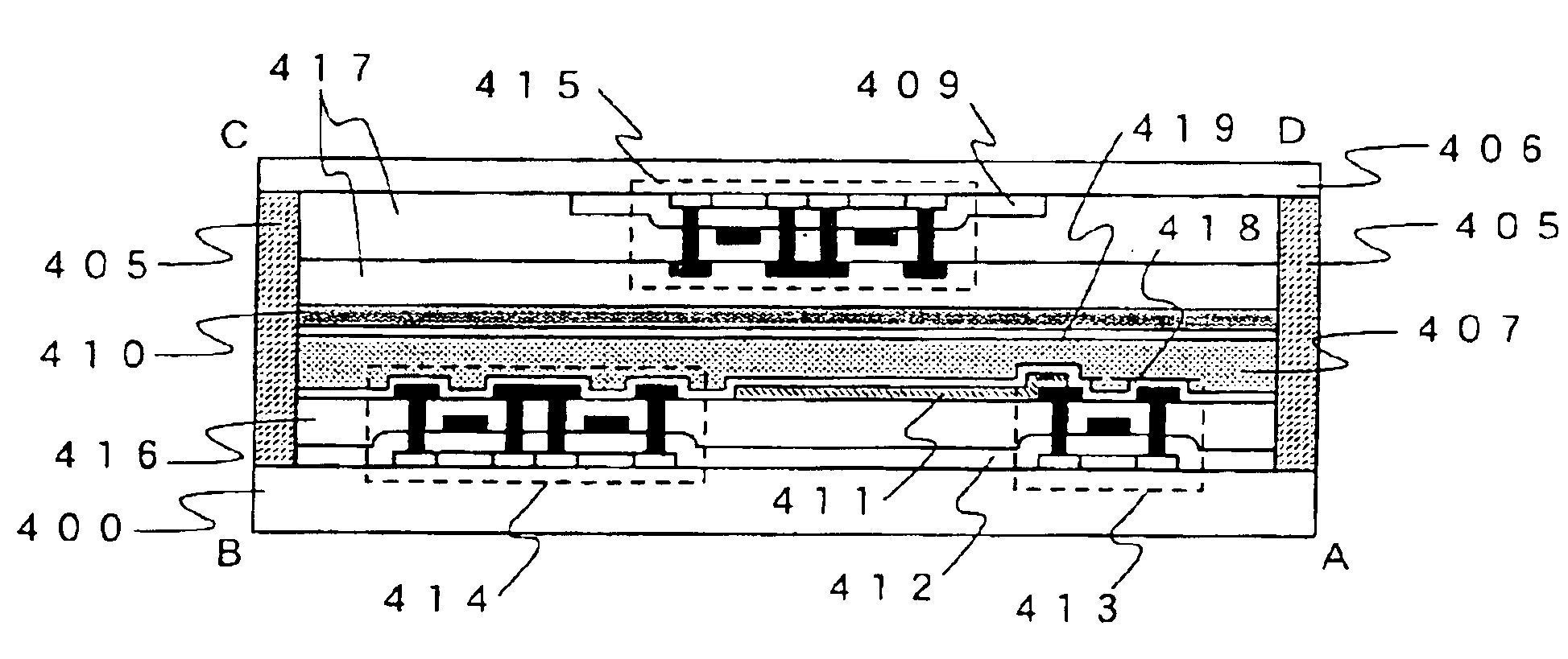
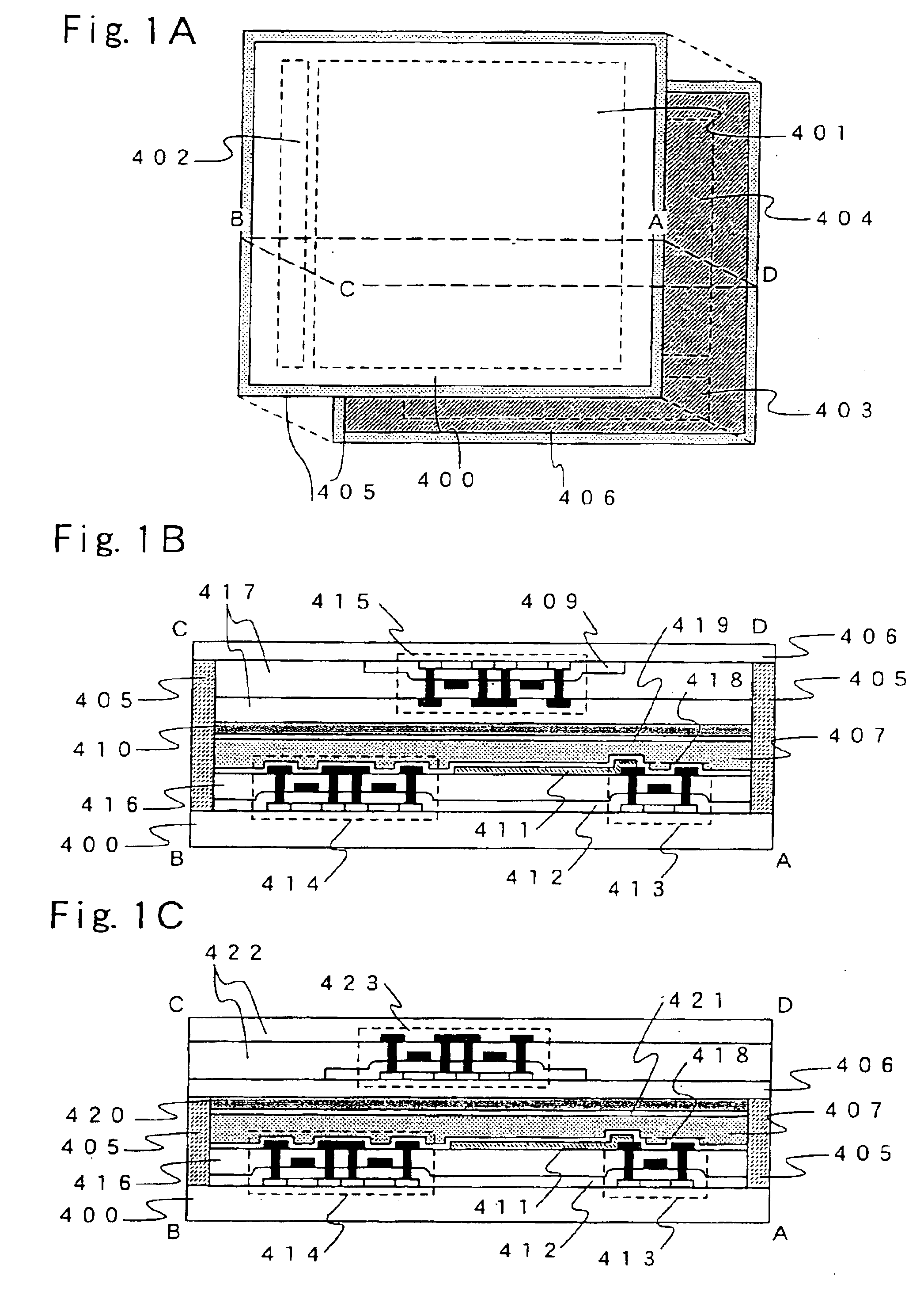
[0075]FIG. 1A is a schematic diagram of a semiconductor device (active matrix semiconductor display device) having an active matrix liquid crystal display portion in which a liquid crystal layer is sandwiched by a glass substrate (pixel substrate) 400 and an opposing substrate 406. A pixel region 401 and a gate signal line driver circuit 402 are formed on the glass substrate 400 in FIG. 1A, and a source signal line driver circuit 403 and a logic circuit 404 are formed on the opposing substrate 406. Further, FIG. 1B is a cross sectional diagram of a surface ABCD of FIG. 1A.

[0076]A sealing agent 405 is formed in FIG. 1B so as to surround the pixel region 401 and the gate signal line driver circuit 402 formed on the glass substrate 400, and the source signal line driver circuit 403 and the logic circuit 404 formed on the opposing substrate 406. Liquid c...

embodiment mode 2

[0097]Formation of TFTs on a glass substrate is mainly performed by using amorphous silicon or polysilicon as an active layer. From the standpoint of high speed operation of logic circuits, it is preferable that the TFT electric field mobility be high, and therefore it is preferable that logic circuits be formed by using polysilicon TFTs rather than amorphous TFTs. On the other hand, it is preferable that amorphous TFTs formed by simple processes and at low cost be used for cases in which high speed operation of logic circuits is not necessary.

[0098]For example, it is preferable that amorphous TFTs be used provided that the gate signal line driver circuit and the source signal line driver circuit are not formed integrally on a substrate used for forming pixels, while it is preferable that polysilicon TFTs be used if the gate signal line driver circuit and the source signal line driver circuit are formed as integrated on the pixel substrate. As an example of an integral formation, a ...

embodiment mode 3

[0100]A semiconductor device of the present invention can employ optimal TFT structures and circuit specification respectively for a pixel substrate and an opposing substrate because pixels and logic circuits are manufactured on different substrates. An embodiment in which the TFT structure and the circuit driver voltage differ between logic circuits on an opposing substrate and logic circuits on a pixel substrate is explained in Embodiment Mode 3.

[0101]It is necessary for a pixel region and a driver circuit for driving pixels to use an electric power source voltage that is higher than the voltage required by elements, and therefore a voltage higher than that required by logic circuits is often employed. For example, a voltage on the order of 16 V is needed for a liquid crystal display portion, and a voltage on the order of 12 V becomes necessary for an EL display portion, while an electric power source of between 3 V and 5 V is needed by the logic circuits.

[0102]Different electric ...


PUM

PropertyMeasurementUnit
angleaaaaaaaaaa
operating frequencyaaaaaaaaaa
voltageaaaaaaaaaa

Abstract

A semiconductor device reduced in size is provided in which the surface area outside of a display portion required for IC chips to mounted is reduced in a semiconductor device having an active matrix display portion. Further, signal wiring connection defects that accompany IC chip mounting are reduced. By manufacturing TFTs on an opposing substrate in a reflecting active matrix semiconductor device, thus manufacturing a desired logic circuit, the logic circuit, conventionally mounted externally, is formed on the opposing substrate. Further, the semiconductor device is made high speed and high performance by using suitable TFT structures and electric power source voltages for pixels and driver circuits on a pixel substrate and for the logic circuit on the opposing substrate.

Description

BACKGROUND OF THE INVENTION[0001]1. Field of the Invention[0002]The present invention relates to a semiconductor device in which thin film transistors (hereinafter referred to as TFTs) are formed on a substrate having an insulating surface. In particular, the present invention relates to a liquid crystal display device having an active matrix display portion, an EL display device, and other active matrix display devices.[0003]2. Description of the Related Art[0004]The development of electronic equipment having mounted semiconductor devices therein, in particular semiconductor display devices, has been remarkable in recent years. There are many examples of such applications, including portable equipment like game machines, notebook personal computers, and portable telephones, liquid crystal televisions, liquid crystal displays (liquid crystal display devices), and OLED displays (EL display devices). Semiconductor devices and semiconductor display devices can be made lighter and thinn...

Claims


Application Information

Patent Timeline
Patent Type & Authority Patents(United States)
IPC IPC(8): G02F1/13G02F1/1362H01L21/70H01L21/84H01L27/12H01L27/06G02F1/1333H01L21/77
CPCG02F1/13454H01L27/1214H01L27/0688G02F2001/133368G02F1/133368
Inventor KATO, KIYOSHIOZAKI, TADAFUMIMUTAGUCHI, KOHEI
Owner SEMICON ENERGY LAB CO LTD
Why Eureka
Try Eureka