High performance CMOS device structure with mid-gap metal gate

a metal gate and high-performance technology, applied in the direction of semiconductor devices, electrical devices, transistors, etc., can solve the problems of unacceptably high threshold voltage vt for both the pfet area and the nfet area, reduce diffusion, and improve the effect of short channel

Inactive Publication Date: 2005-07-12
IBM CORP
View PDF21 Cites 141 Cited by
  • Summary
  • Abstract
  • Description
  • Claims
  • Application Information

AI Technical Summary

Benefits of technology

[0008]The present invention provides high performance (surface channel) CMOS devices with a mid-gap work function metal gate, and is applicable to 0.1 um technology structures. Pursuant to the present invention, an epitaxial layer is used for a threshold voltage Vt adjust / decrease for the PFET area, for large Vt reductions (˜500 mV), as are required by CMOS devices with a mid-gap metal gate. The present invention provides counter doping using an in situ boron (B) doped epitaxial layer or a B and carbon (C) co-doped epitaxial layer, wherein the C co-doping provides an additional degree of freedom to reduce the diffusion of B (also during subsequent activation thermal cycles) to maintain a shallow B profile, which is critical to provide a surface channel CMOS device with a mid-gap metal gate while maintaining good short channel effects. The present invention produces B diffusion profiles in an epitaxial layer of B doped silicon or B and C co-doped silicon on the PFET area of the CMOS devices. The B diffusion profiles are satisfactorily shallow, sharp and have a high B concentration for devices with mid-gap metal gates, to provide and maintain a thin, highly doped B layer under the gate oxide.
[0009]A further object of the subject invention is the provision of a method of fabricating mid-gap metal gate CMOS devices with good short channel effects wherein an epitaxial layer is used for a threshold voltage Vt adjust / decrease for the PFET area, for large Vt reductions (˜500 mV), as are required by CMOS devices with a mid-gap metal gate.

Problems solved by technology

In the fabrication of high performance CMOS devices with ultra-thin gate dielectrics and polysilicon gates, the depletion layer formed in the polysilicon gate in inversion bias becomes a significant fraction of the gate capacitance and degrades the device performance.
However, this approach adds significant cost and complexity to the process.
For CMOS mid-gap workfunction metal gates, the threshold voltage Vt for both the PFET area and the NFET area become unacceptably high.

Method used


Image

  • High performance CMOS device structure with mid-gap metal gate
  • High performance CMOS device structure with mid-gap metal gate
  • High performance CMOS device structure with mid-gap metal gate

Examples


Embodiment Construction

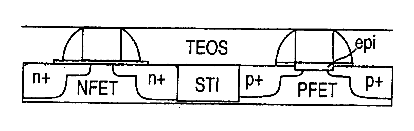
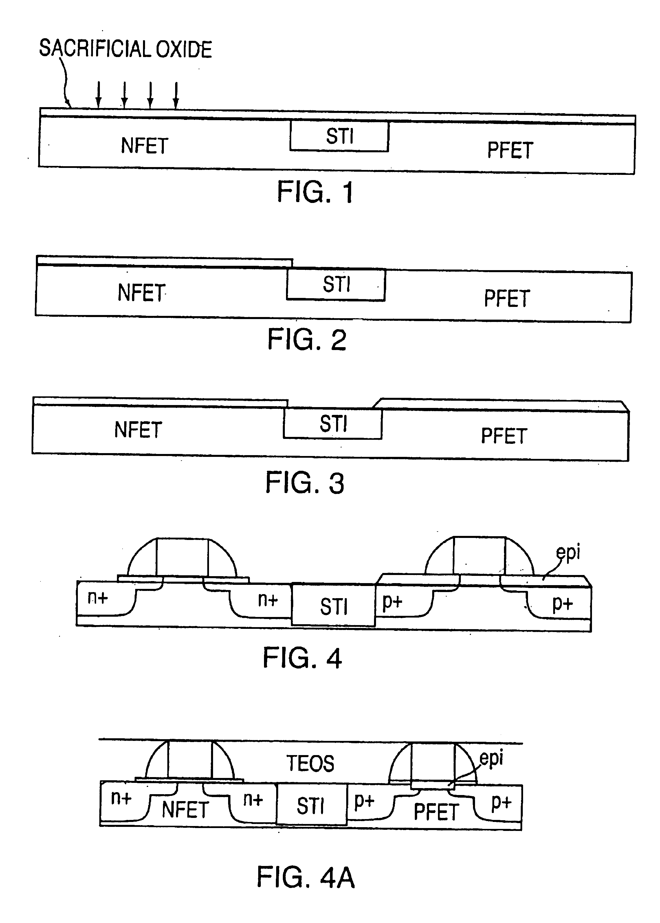
[0023]The present invention provides a method for fabricating high performance CMOS devices with a mid-gap workfunction metal gate. The present invention uses the same metal with a mid-gap work function for the gate of both the PFET area and NFET area, and provides a device structure and fabrication method for CMOS devices with a mid-gap workfunction metal gate with an approximately 40 nm gate length.

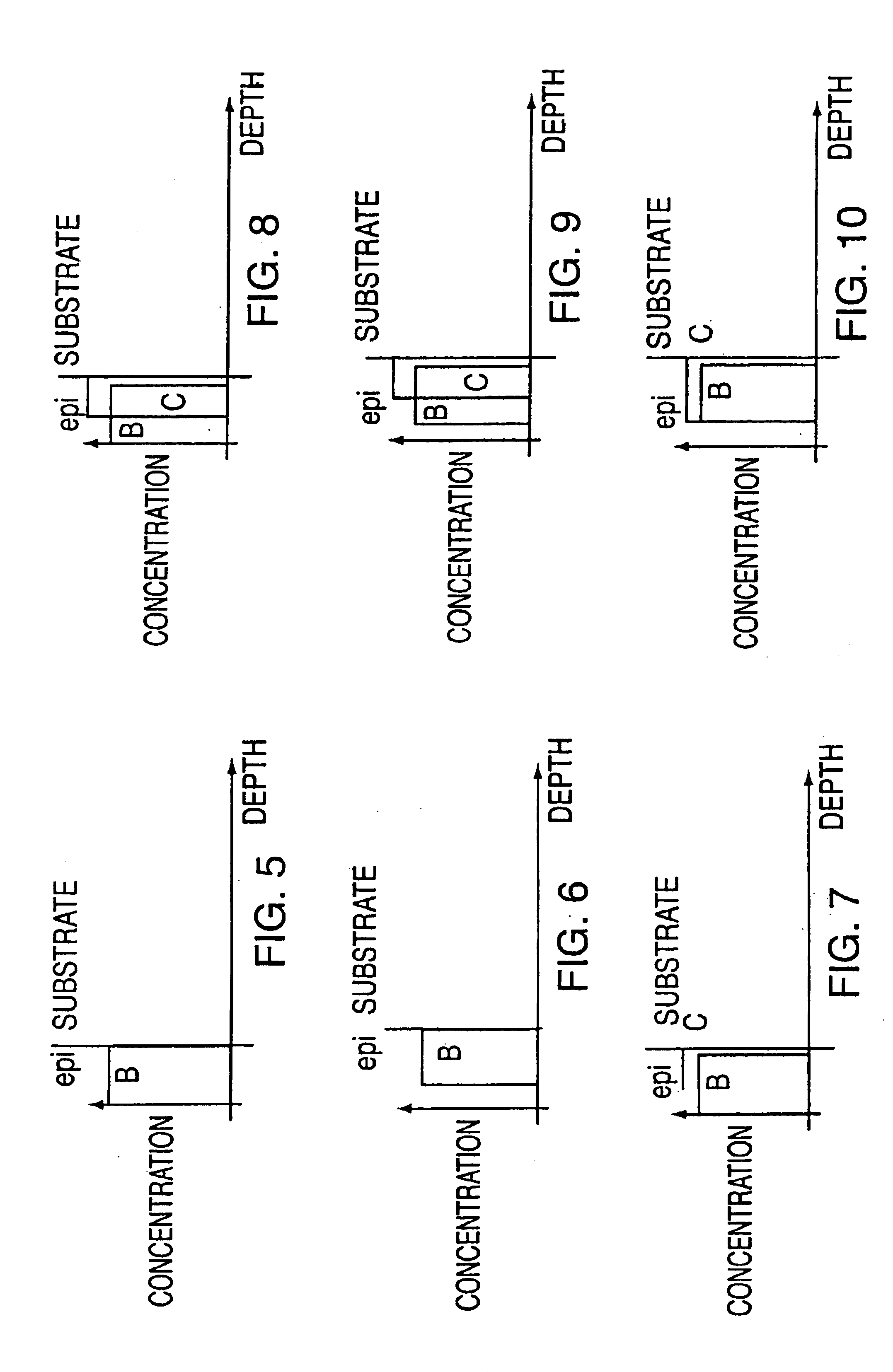
[0024]For CMOS devices with a mid-gap workfunction metal gate, the threshold voltage Vt for both the PFET area and the NFET area become unacceptable high. The threshold voltage has to be adjusted downwardly by implanting a p-type dopant into the surface of the PFET area and an n-type dopant into the surface of the NFET area. Ideally the dopant should be positioned right at the gate dielectric / silicon interface such that large shifts in the threshold voltage Vt are possible but short channel effects are not degraded. In practice this counter doping layer can have a finite thickness befor...


PUM

PropertyMeasurementUnit
threshold voltageaaaaaaaaaa
gate lengthaaaaaaaaaa
mid-gap work functionaaaaaaaaaa

Abstract

High performance (surface channel) CMOS devices with a mid-gap work function metal gate are disclosed wherein an epitaxial layer is used for a threshold voltage Vt adjust / decrease for the PFET area, for large Vt reductions (˜500 mV), as are required by CMOS devices with a mid-gap metal gate. The present invention provides counter doping using an in situ B doped epitaxial layer or a B and C co-doped epitaxial layer, wherein the C co-doping provides an additional degree of freedom to reduce the diffusion of B (also during subsequent activation thermal cycles) to maintain a shallow B profile, which is critical to provide a surface channel CMOS device with a mid-gap metal gate while maintaining good short channel effects. The B diffusion profiles are satisfactorily shallow, sharp and have a high B concentration for devices with mid-gap metal gates, to provide and maintain a thin, highly doped B layer under the gate oxide.

Description

[0001]The present application is a divisional of U.S. patent application Ser. No. 10 / 127,196 filed on Apr. 19, 2002 now U.S. Pat. No. 6,762,469.BACKGROUND OF THE INVENTION[0002]1. Field of the Invention[0003]The present invention relates generally to high performance CMOS device structures with a mid-gap metal gate, and more particularly pertains to high performance CMOS device structures with a mid-gap work function metal gate wherein an epitaxial layer is used for a threshold voltage Vt adjust / decrease for the PFET area, for large Vt reductions (˜500 mV), as are required by CMOS devices with a mid-gap metal gate.[0004]2. Discussion of the Prior Art[0005]The problems and issues associated with the design of CMOS devices with a mid-gap work function metal gate are well known and recognized in the prior art (e.g. E. Josse and T. Skotnicki, IEDM 1999).[0006]In the fabrication of high performance CMOS devices with ultra-thin gate dielectrics and polysilicon gates, the depletion layer f...

Claims


Application Information

Patent Timeline
Patent Type & Authority Patents(United States)
IPC IPC(8): H01L21/70H01L21/8238H01L29/423H01L27/092H01L29/49
CPCH01L21/823807H01L21/823828
Inventor MOCUTA, ANDA C.IEONG, MEIKEIAMOS, RICKY S.BOYD, DIANE C.MOCUTA, DAN M.CHEN, HUAJIE
Owner IBM CORP
Why Eureka
Try Eureka